
Chapter 6: GPU and GPU-Related Optimization
Learning Objectives
Before diving into specific analysis, let's clarify this section's focus. This section covers the hardware accelerators that LLM training and inference depend on:
- Understand GPU basic architecture, differences from CPU, and the evolution from graphics processor to AI engine
- Master GPU execution model (SM, Warp, Block, Thread) and hierarchical memory model (global memory, L2 cache, shared memory, registers, etc.)
- Learn key GPU performance optimization techniques: avoiding serial execution, low-precision computation, operator fusion, recomputation, memory coalescing, tiling, etc.
- Deeply understand FlashAttention (V1/V2/V3) and PagedAttention core principles and their improvements for long-sequence training and inference
- Understand domestic GPUs (Huawei Ascend, Baidu Kunlun, Haiguang, Moore Threads, Alibaba T-Head, etc.) product performance, software ecosystem, and market status
After completing this chapter, you will be able to: systematically understand GPU hardware architecture and execution model, master key performance tuning techniques from memory optimization to operator fusion, deeply grasp how FlashAttention and PagedAttention break through memory and computation bottlenecks, and form a comprehensive understanding of the domestic AI chip competitive landscape and technology roadmap — enabling rational hardware selection and optimization decisions in actual LLM training and inference tasks.
6.1 GPU Origins: Graphics Processor
Before deep learning became popular, GPUs were seen by ordinary people as gaming graphics cards — graphics processors. Let's use an example to illustrate the difference between GPU and CPU.
When we open a 3D model in a game, we can see that 3D models are composed of many small triangles. A triangle is made of three lines. To save storage space, we only store the three vertex coordinates of each triangle; the pixel coordinates that form the lines are not stored but computed in real-time.
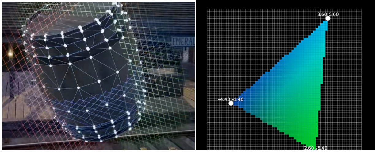
From two points forming a line, we can see that a line only stores two endpoint coordinates, while the intermediate pixels are computed and rendered in real-time. From two vertex coordinates, we can calculate slope and intercept, then determine the positions of points along the line. These are all simple calculations — only lots of simple multiplications and additions. But CPUs are inherently designed for complex logic and can only compute sequentially, so computation time is very long.
People then thought of creating computing units capable of massively parallel simple multiplication and addition — this is the GPU. CPU and GPU have no superiority or inferiority; they are simply units designed to execute different functions. GPU computing units are called CUDA Cores.
6.1.1 CPU (Central Processing Unit) vs GPU (Graphics Processing Unit)
The CPU is the execution model we first encountered. Programs run sequentially, executing instructions step by step in a single thread. Supporting this execution model requires large control units and fast execution capabilities because there are many branches and conditional control logic. Therefore, CPUs allocate large chip area to branch prediction (see the figure below); although core count is limited, execution speed is extremely fast. In contrast, GPUs have massive numbers of compute units (ALUs) — those little green squares. Only a tiny portion of chip area is used for control logic, using minimal control logic to coordinate massive parallel compute units. Conceptually, this reflects the different emphases of CPU and GPU.
The two have fundamentally different design goals. CPU optimizes for latency, pursuing fastest single-task completion. GPU optimizes for throughput — GPU doesn't care about individual task latency, only pursuing fastest overall completion of all tasks. To this end, GPU is equipped with many threads that can quickly sleep and wake. Although GPU has higher per-task latency, overall completion time beats CPU. This is their different design philosophy and goals. Therefore, GPU architecture differs in that GPU runs many Streaming Multiprocessors (SMs).
CPU is designed to minimize single-task latency, respond quickly to complex logic, with most transistors used for control logic and cache. Core count is typically 4-64, capable of out-of-order execution, branch prediction, speculative execution, etc.
GPU is designed to maximize data throughput, batch-process simple computations, with most transistors used for Arithmetic Logic Units (ALUs). Cores are numerous but simple, reaching tens of thousands. It optimizes for throughput, pursuing fastest overall completion of all tasks. Equipped with large control units and branch predictors, core count is low (4-32) but clock frequency is extremely high.
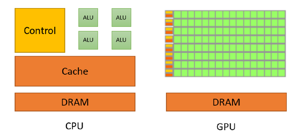
From the figure above we can see: CPU's compute units (green portion) are few; most area is used for Control and Cache, which determines its ability for complex logical operations. GPU is different — its control unit is small (yellow portion); most area consists of green compute units, which determines its ability for massively parallel simple multiplication and addition, but not complex logic or computation. GPU primarily optimizes throughput, pursuing fastest overall completion of all tasks. Control logic occupies only a tiny fraction of chip area, while compute units (ALUs) occupy the vast majority. So when using GPU, we still need CPU scheduling — a good GPU needs a good CPU to function well.
In the AI era, matrices in deep learning pushed GPU to prominence. Because the core of the AI era is neural network computation, which involves massive matrix operations. The essence of matrix operations is lots of multiplication and addition, perfectly suited for GPU's simple and repetitive computation style. Around 2010, people began using GPUs for AI-related computation.
6.1.2 GPU Evolution: From Graphics Chip to AI Engine
1. The Dawn of Graphics Display (Pre-1980s)
The era without GPU: Computer graphics relied entirely on CPU computation. 1981: IBM PC's CGA display card could only show 16 colors, like an "electronic photo frame" — all computation done by CPU. 1987: IBM introduced the VGA standard, capable of displaying 256 colors, but still purely "display" functionality with no compute capability.
Key breakthrough: In 1985, ATi was founded, beginning to use ASIC technology for graphics chips. In 1992, ATi's Mach32 graphics card first integrated graphics acceleration functionality — this was the "embryo" of GPU.
2. The 3D Accelerator Card Battleground (1990s)
The 90s were the golden age of "graphics accelerators," but the formal name "GPU" didn't exist yet.
Milestone events: 1994, 3DLabs released Glint300SX — the first PC 3D acceleration chip was born; 1996, 3dfx's Voodoo chip enabled ordinary PCs to run 3D games, ushering in the consumer 3D era; 1997, Fujitsu released the first 3D geometry processor for personal computers, and Mitsubishi introduced a chip supporting Transform and Lighting (T&L).
But standards were chaotic and mutually incompatible; chips could only handle specific 3D tasks with very "specialized" functionality; at the time they were called "3D accelerator cards" — the GPU concept didn't exist yet.
3. GPU Officially Born: NVIDIA's Counterattack (1999-2006)
1999, NVIDIA released the GeForce 256, first proposing the "GPU" (Graphics Processing Unit) concept. This name distinguished it from traditional CPU, declaring: graphics cards now have their own brain.
The GeForce 256 was revolutionary: Hardware T&L technology liberated 3D graphics coordinate transformation and lighting computation from CPU, making them GPU-specialized tasks. It achieved single-chip integration, combining triangle assembly, clipping, texturing, and rendering functions, and delivered performance leap: reducing CPU's 3D computation burden by over 80%.
In 2000, a major market reshuffle occurred. After 2000, old players like 3dfx and Matrox gradually withdrew, leaving only NVIDIA GeForce and ATI Radeon in a duopoly (ATI was acquired by AMD in 2006).
4. The Programmable Era (2001-2012)
Phase 1: Fixed Pipeline Shaders (2001-2006)
2001, Microsoft DirectX 8 introduced vertex shaders and pixel shaders — GPUs could now run simple programs. Previously, GPUs were like "screw-tightening workers" on a fixed assembly line; now they became "small robots" capable of executing simple instructions.
Phase 2: Unified Shader Architecture (2006-2012)
2006, NVIDIA released the GeForce 8800 GTX (G80 core), the first unified shader architecture GPU. Previously, vertex shaders and pixel shaders were separate "specialists"; now they became general-purpose "general practitioners." Compute resources could be dynamically allocated, utilization rose from 50% to 90%+. Simultaneously, CUDA technology was released, enabling GPUs to run C language programs.
| Architecture Year | Core Breakthrough | Representative Product |
|---|---|---|
| Tesla (2006) | Introduced CUDA, opened GPGPU era | GTX 280 |
| Fermi (2010) | Supported double-precision computation, ECC error correction | GTX 480 |
| Kepler (2012) | Dynamic parallelism, high energy efficiency | GTX 680 |
5. General-Purpose Computing Era: GPU Transforms into "Supercomputing Core" (2012-2018)
2012 was the turning point: AI researchers used GPUs to train deep neural networks, and AlexNet's image recognition accuracy shocked the world. From then on, GPU upgraded from "gaming graphics card" to "AI engine."
NVIDIA built the NVIDIA CUDA ecosystem, enabling programmers to easily harness GPU compute power.
6.1.3 A100 GPU Core Architecture
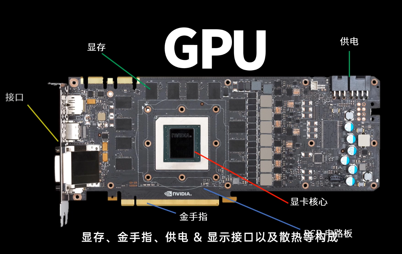
An NVIDIA GPU card cross-section is shown in the figure. A graphics card consists of power supply, GPU core, video memory (VRAM), display interface, and PCIe connector (gold finger).
We primarily focus on the GPU core: the GPU core is composed of CUDA cores, control units, and cache units. The biggest difference between CPU and GPU is that GPU's work is mostly repetitive 3D modeling or rendering, and the streaming processors handle vertex computation or pixel computation, dynamically allocating the number of streaming processors for vertex vs. pixel computation to achieve efficient resource utilization.
A100 is NVIDIA's pure-compute GPU designed for data centers, with no graphics output capability.
Layer 1: Product Form
PCIe version (common form factor) Dimensions: dual-slot full-height, 267mm long. Power: 250W (40GB version) / 300W (80GB version). Cooling: passive cooling, fanless (relies on server airflow). Interface: PCIe 4.0 x16 gold finger + NVLink bridge connector; Weight: approximately 1.4 kg.
Layer 2: PCB Board-Level Components
GA100 GPU Core Chip
Package: Massive BGA package, approximately 55mm×55mm. Position: center of the board, soldered to PCB. 54.2 billion transistors, 7nm process, 826mm² area.
HBM2e Memory Stacks (Revolutionary Design) Unlike consumer-grade GPU's GDDR memory chips, A100 uses 3D stacking technology:
┌───────────────────────────────────────────┐
│   HBM2e Memory Stack (8 layers)            │ ← Like a "chip skyscraper"
│  ┌───────┐┌───────┐┌───────┐               │
│  │ DRAM  ││ DRAM  ││ DRAM  │               │ ← 8Gb per layer
│  └───────┘└───────┘└───────┘               │
│      Through-Silicon Via (TSV) vertical     │
│                GPU SoC                     │
└───────────────────────────────────────────┘
Layer 3: GA100 GPU Core Architecture (Chip Internal Macro Structure)
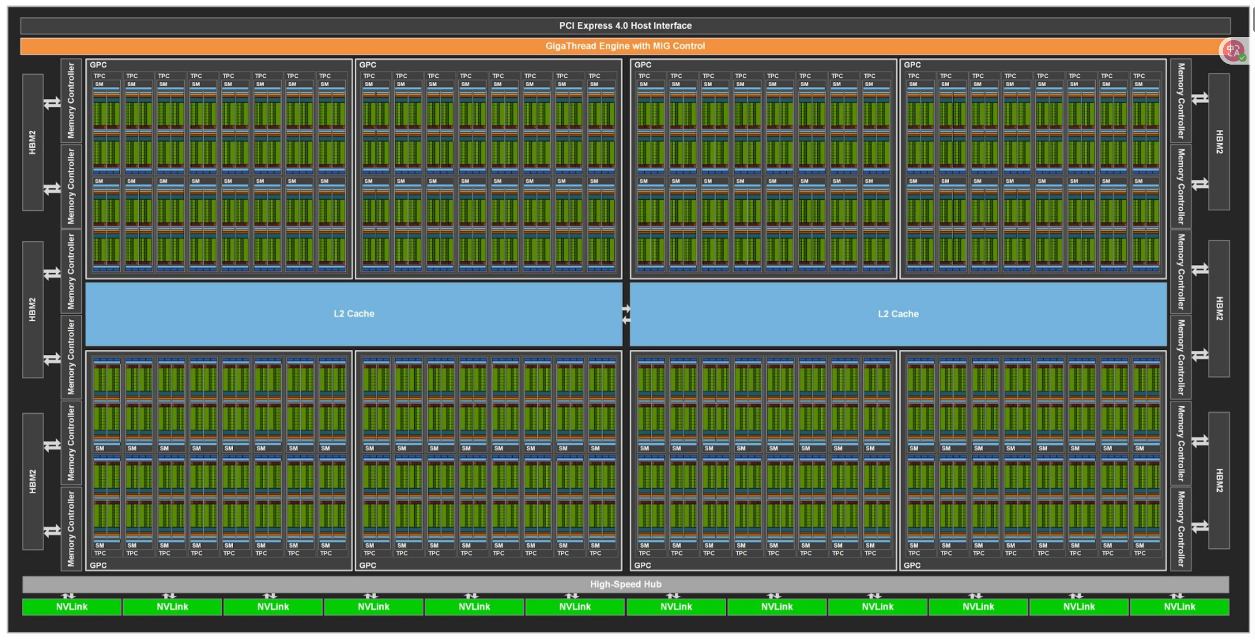
Ampere architecture topology:
┌─────────────────────────────────────────────────────┐
│                    GA100 GPU Core                    │
│                                                      │
│  ┌─────────┐  ┌─────────┐  ┌─────────┐              │
│  │  GPC 0  │  │  GPC 1  │  │  GPC 2  │              │
│  │ (12 TPC)│  │ (12 TPC)│  │ (12 TPC)│              │
│  └─────────┘  └─────────┘  └─────────┘              │
│                                                      │
│  ┌─────────┐  ┌─────────┐  ┌─────────┐              │
│  │  GPC 3  │  │  GPC 4  │  │  GPC 5  │              │
│  │ (12 TPC)│  │ (12 TPC)│  │ (12 TPC)│              │
│  └─────────┘  └─────────┘  └─────────┘              │
│                                                      │
│  ┌─────────┐  ┌─────────┐  ┌─────────┐              │
│  │  GPC 6  │  │  GPC 7  │  │  GPC 8  │              │
│  │ (12 TPC)│  │ (12 TPC)│  │ (12 TPC)│              │
│  └─────────┘  └─────────┘  └─────────┘              │
│                                                      │
│  HBM2e Controllers ×8    ┌──────────────────┐        │
└───────────────────────────│  PCIe 4.0 ×16     │────────┘
                            └──────────────────┘
A100 has four levels of architectural topology: first, GPC (Graphics Processing Cluster) — a GPU core has 8 (7-8 actually enabled) GPCs; each GPC has 12 TPCs (Texture Processing Clusters), totaling 96 TPCs; each TPC has 2 SMs (Streaming Multiprocessors), totaling 192 SMs (108 actually enabled); each SM has 64 CUDA Cores, totaling 192 × 64 = 6,912 CUDA Cores.
Then there are Tensor Cores: each SM has 4 (432 third-gen Tensor Cores actually enabled).
Layer 4: SM (Streaming Multiprocessor) Internal Structure
A100's SM is the Ampere architecture core, fundamentally enhanced compared to consumer-grade GPUs:
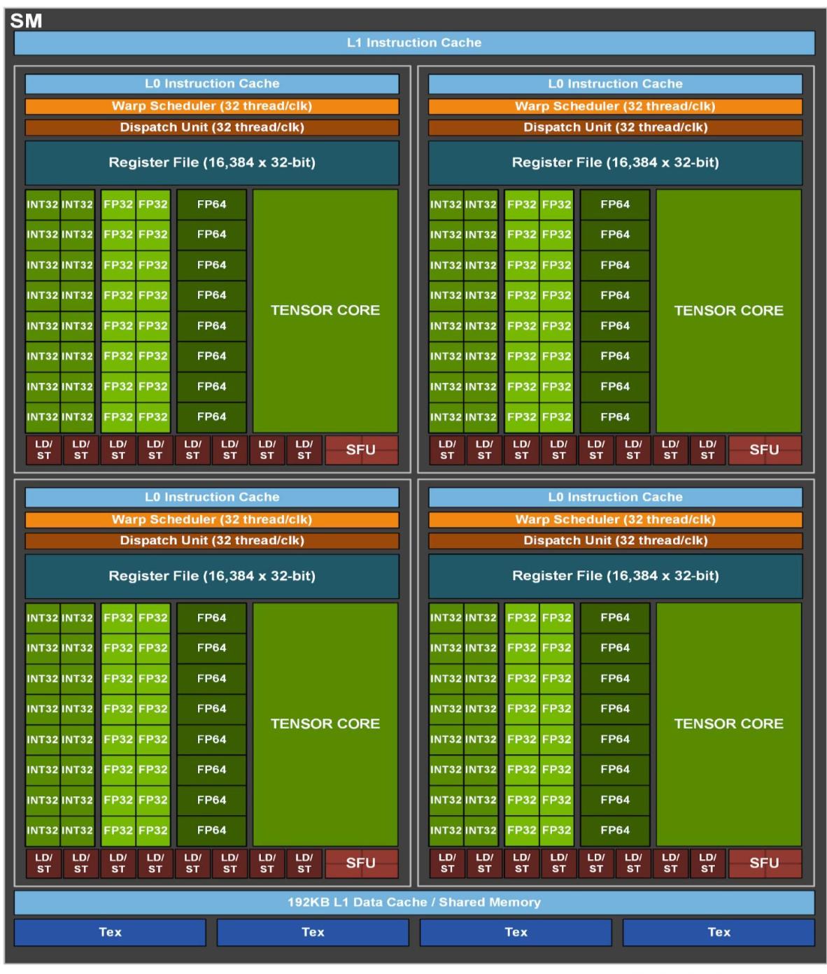
┌──────────────────────────────────────────────┐
│              SM (Streaming Multiprocessor)     │
│                                               │
│  ┌────────┐ ┌────────┐ ┌────────┐            │
│  │CUDA Core│ │CUDA Core│ │CUDA Core│           │
│  │  ×64   │ │  ×64   │ │  ×64   │ ← FP32/INT32│
│  └────────┘ └────────┘ └────────┘            │
│                                               │
│  ┌──────────────────────────┐                 │
│  │  3rd-Gen Tensor Core ×4  │ ← AI-specialized│
│  │  FP64/TF32/FP16/INT8     │   accelerator   │
│  └──────────────────────────┘                 │
│                                               │
│  ┌──────────────────────────┐                 │
│  │   Shared Memory / L1     │ ← 192KB         │
│  │        128KB             │                 │
│  └──────────────────────────┘                 │
│                                               │
│  ┌──────────────────────────┐                 │
│  │   Register File          │ ← 256KB         │
│  │        256KB             │                 │
│  └──────────────────────────┘                 │
└──────────────────────────────────────────────┘
What makes SM unique is the CUDA Cores: 64 per group, 4 groups = 256 CUDA Cores/SM (actual configuration: 64 FP32 + 64 INT32). Also has 3rd-gen Tensor Cores, supporting structured sparsity (2× performance) and FP64 double precision (absent in consumer GPUs).
Layer 5: Tensor Core Performance
| Data Type | Performance (per GPU) | Use Case |
|---|---|---|
| FP64 | 19.5 TFLOPS | Scientific computing, high-precision AI |
| TF32 | 156 TFLOPS | Default AI training format |
| FP16/BF16 | 312 TFLOPS | Mixed precision training |
| INT8 | 624 TOPS | Inference acceleration |
| INT4 | 1,248 TOPS | Extreme inference optimization |
Core technologies:
- Structured Sparsity: Automatically skips zero-value computation, 2× effective performance boost
- Multi-Precision Fusion: Processes different precision data within a single cycle
6.2 GPU Execution Model: SM (Streaming Multiprocessor)
6.2.1 Core Functions of SM
We can view the Streaming Multiprocessor as an atomic unit (i.e., the smallest unit). When programming with tools like Triton, the operation level corresponds to SMs. Within each SM, it contains many Streaming Processors (SPs), and each streaming processor executes massive numbers of threads in parallel. Think of it this way: the SM has a set of control logic that determines what to execute, such as implementing branch decisions; while SPs apply the same instruction to different data segments. This enables massive parallel computation. Under this architecture, each SM is the basic unit of control granularity, while individual SPs can independently complete large amounts of computation. Taking the previous-generation GPU A100 as an example, it contains 108 SMs — far exceeding most CPUs' core counts. Each SM internally integrates many SPs and dedicated matrix multiplication units — this is the basic form of its computation model. Each SM can control its dedicated components (such as Tensor Cores) for computation.
Thread Scheduling and Execution
The SM simultaneously manages thousands of threads, deciding which thread uses which compute unit at which time. Unlike CPU, it doesn't save large amounts of state per thread — instead, it performs lightweight switching with near-zero overhead.
Instruction Pipeline
The SM internally has 4 independent instruction pipelines, capable of simultaneously issuing 4 different instructions to different Warps per clock cycle.
Data Caching and Sharing
SM has built-in 192KB of L1 cache / shared memory for fast data access by all CUDA cores within the SM, with latency 100× lower than global memory.
6.2.2 Core Execution Model Concepts
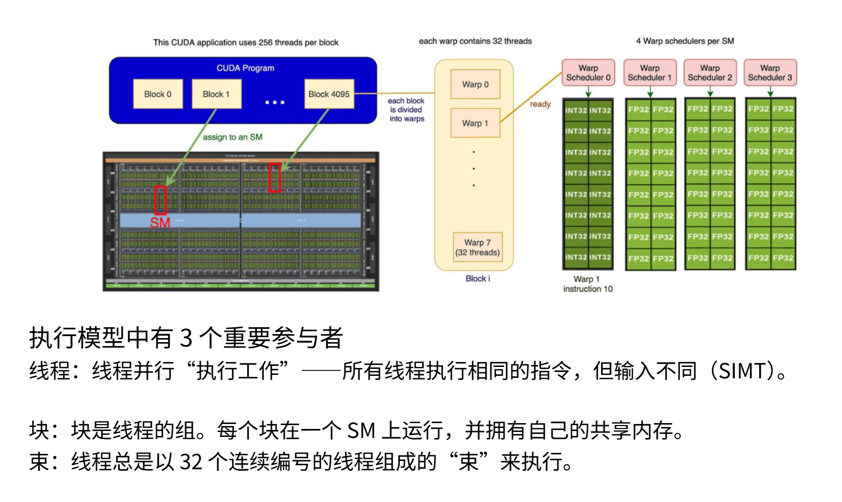
In GPU execution, we think in three granularity levels: Block, Warp, and Thread — in order of progressively finer granularity. A Block is a large thread group, each Block is assigned to one SM for processing. You can think of each SM as an independently working unit, and the Block is the processing unit assigned to it. Within each Block are many threads, each representing a task unit to be executed. These threads run in groups during execution — this grouping is called a Warp. Each Warp consists of 32 consecutively numbered threads, extracted from the Block for synchronous execution. From this diagram we can see: multiple Blocks are assigned to different SMs, each Block contains multiple Warps, and each Warp contains many threads. All these threads execute the same instruction on different data — this is the basic execution model.
1. Warp (Thread Warp)
A Warp is a fixed group of 32 threads, the minimum scheduling unit of the SM. Warp is like a "bus": 32 passengers (threads) must board and alight together, executing exactly the same instruction. If a thread needs to take a different branch (if-else), the entire busload waits — this is called Warp Divergence.
SM simultaneously hosts 64 Warps; 4 Warp schedulers each manage 16 Warps; the 32 threads within a Warp execute synchronously on SIMD units.
2. Block (Thread Block)
Block is a programmer-specified thread group, mapped to 1 SM for execution. Block is like a "construction crew": crew members can share tools (shared memory) and synchronize via signals.
Each Block exclusively occupies the SM's shared memory and register resources; all threads within a Block must execute within the same SM (cannot cross SMs).
3. Thread
Thread is the finest-granularity execution unit. Each thread executes the same Kernel code but operates on different data. Thread is like a "worker on the assembly line," each responsible for one data element (e.g., one number in a vector).
Each thread has private registers (typically 256); thread ID: threadIdx.x determines which data it processes.
4. SIMT (Single Instruction, Multiple Threads)
GPU execution model where multiple threads (Warp) share the same instruction but operate on different data. SIMT is like a "choir": the conductor (instruction) is unified, but each person sings their own part (data).
6.3 GPU Memory Model
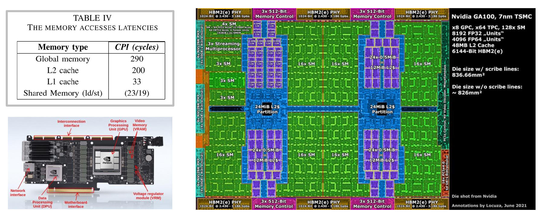
The closer memory is to SM, the faster the access speed. Therefore, there exist extremely high-speed memory types (such as L1 cache and shared memory), located within the SM, with extremely fast read/write speeds. Components like registers that require frequent read/write should be placed in L1 and shared memory.
As shown in the figure, these green regions are SM clusters, while blue regions represent L2 cache adjacent to SMs — though not inside the SM, they are still physically close, with reasonably fast speed (though an order of magnitude slower than L1). Outside the chip (taking this 3090 or PCIe A100 as an example), DRAM memory is physically installed beside the GPU chip, meaning data needs to actually leave the chip through physical connections for transfer. You can see these yellow connectors at the edges of the chip diagram. These are HBM connectors, connecting to DRAM chips physically outside the GPU.
From the left side of the figure above you can see the speed required to access these storage levels. SM-internal storage access is much faster — data can be retrieved in about 20 clock cycles, while accessing L2 cache or global memory requires 200 to 300 clock cycles. This 10× difference severely impacts performance. If a computation segment requires global memory access, it may mean your SM has no work to do — matrix multiplications all completed, tasks exhausted, just spinning idle. This results in low utilization. In some sense, this becomes the core theme for thinking about memory architecture and the key to understanding how GPUs work.
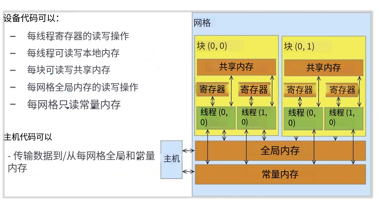
Starting with registers — these are extremely fast storage units for holding single numeric data values. Then local memory, shared memory, and global memory — they progressively increase in the memory hierarchy and get progressively slower.
Code can write to global memory, and can also write to constant memory (though less commonly used). Each thread can access its own registers and shared memory, but information across thread blocks needs to be written to global memory. This means when writing threads that execute tasks, ideally they should operate on the same small batch of data so they don't need to cross threads. We can load this small batch into shared memory, where all threads can efficiently access it, and the task completes after execution. This is the ideal execution pattern. Conversely, if threads need to access data everywhere, they must access global memory, which is very, very slow.
6.3.1 Layer 1: Global Memory (HBM)
| Property | Parameter / Description |
|---|---|
| Physical Location | HBM2e memory stacks outside GPU chip |
| Capacity | A100: 40GB/80GB |
| Bandwidth | 2,039 GB/s (A100) |
| Latency | ~500 GPU cycles (~250ns) |
| Programming Control | Manual (cudaMalloc) |
| Visibility | All threads accessible |
Global memory stores all model weights, activations, gradients (e.g., GPT-3's 175 billion parameters); training data, intermediate results, final output — achieving data persistence; we copy data from host memory via PCIe — the CPU-GPU transfer channel.
Global memory provides massive capacity (80GB), capable of holding large models' enormous memory requirements; cost is relatively low (HBM2e is expensive but 100× cheaper than SRAM) — it is the foundation of GPU storage.
6.3.2 Layer 2: L2 Cache (Level 2 Cache)
| Property | Parameter / Description |
|---|---|
| Physical Location | Inside GPU chip, shared by all SMs |
| Capacity | 40MB (A100) |
| Bandwidth | ~3TB/s |
| Latency | ~200 cycles (~100ns) |
| Programming Control | Automatic (hardware-controlled) |
| Visibility | All SMs, all threads |
Accelerates global data by automatically caching hot data from global memory (e.g., frequently accessed model weights); serves as data sharing hub — SMs exchange data via L2 cache (3× faster than going directly through HBM); provides data consistency guarantee — all SMs see consistent L2 data.
Alleviates memory bandwidth bottleneck — AI training spends 90% of time accessing the same weights, L2 cache hits can save 95% of HBM bandwidth; hardware automatic management — no programmer intervention needed, reducing programming complexity.
6.3.3 Layer 3: L1 Cache / Shared Memory
| Property | Parameter / Description |
|---|---|
| Physical Location | Inside each SM |
| Capacity | 192KB/SM (A100, configurable) |
| Bandwidth | 1TB/SM |
| Latency | 20-40 cycles (~10-20ns) |
| Programming Control | Fully manual (__shared__) |
| Visibility | All threads within a Block |
It is a thread collaboration warehouse — Block threads exchange data through shared memory (e.g., matrix multiplication tiling data); enables manual performance optimization — hot data can be explicitly placed into shared memory for near-register speed; L1 cache function — when not manually used, automatically serves as L1 cache for global memory data.
L1 speed is 5× faster than L2 — the core battlefield of GPU performance optimization; flexibility — high programmer control enabling complex algorithms (reduction, scan, convolution); cost-effectiveness: 192KB/SM × 108 SM = 20MB total capacity, cheaper than pure SRAM L2.
6.3.4 Layer 4: Constant Memory
| Property | Parameter / Description |
|---|---|
| Physical Location | Dedicated cache inside chip |
| Capacity | 64KB (global constant) |
| Bandwidth | Broadcast mechanism (1 read serves 32 threads) |
| Latency | ~5 cycles (cache hit) |
| Programming Control | Read-only, __constant__ declaration |
| Visibility | All GPU threads, read-only |
Stores broadcast data — when all threads in a Warp read the same constant (e.g., neural network learning rate), only 1 memory access needed; stores configuration parameters — Kernel call parameters, lookup tables, constant coefficients.
Features extreme energy efficiency — broadcast saves 99% bandwidth; dedicated cache — doesn't consume L1/L2 resources.
6.3.5 Layer 5: Register File
| Property | Parameter / Description |
|---|---|
| Physical Location | Inside SM, beside each CUDA core |
| Capacity | 256KB/SM (A100) |
| Bandwidth | 10TB/SM (theoretical) |
| Latency | 1 cycle (zero overhead) |
| Programming Control | Fully automatic (compiler-allocated) |
| Visibility | Thread-private |
Register file enables zero-latency computation, storing thread local variables and temporary results. Achieves extreme parallelism — 255 registers per thread, supporting deep pipelining.
Register file characteristics: fast speed — 1 cycle latency. But expensive — register file capacity is small. Its capacity limit determines parallelism — the fewer registers used, the more Warps an SM can host.
6.3.6 Why So Many Memory Layers in GPU?
1. Speed and Capacity Cannot Coexist
| Memory Type | Speed | Capacity | Cost ($/GB) (estimated) |
|---|---|---|---|
| Registers | 1 cycle | 256KB/SM | $1,000,000 |
| Shared Memory | 20 cycles | 192KB/SM | $100,000 |
| L2 Cache | 200 cycles | 40MB | $10,000 |
| HBM2e VRAM | 500 cycles | 80GB | $100 |
If we only used registers, 80K units wouldn't be enough to build one card; if we only used VRAM, 90% of compute power would be wasted. Hierarchical design is the only economically viable solution. It's a compromise among speed, capacity, and cost.
2. Generality vs. Specialization Trade-off
Global memory is a general warehouse — it stores everything but is slow. Shared memory is a specialized warehouse — programmers precisely control it with extremely fast speed. L1/L2 are automatic caches — hardware intelligently predicts, no programming needed.
3. Locality Principle and Parallel Computing
Recently accessed data is likely to be accessed again (e.g., weights in a loop) — placing this in global memory would be very expensive. There's also spatial locality — adjacent data is likely accessed together (e.g., elements in the same matrix row).
GPU's solution is hierarchical: L2 cache exploits temporal locality, caching repeatedly accessed weights; shared memory exploits spatial locality, manually loading tiling data; Warp exploits constant memory's broadcast特性, 1 read serving 32 threads. We'll cover more later.
GPU Memory vs CPU Memory: Essential Differences
The table below illustrates the differences between GPU and CPU:
| Property | GPU (A100) | CPU (Xeon) |
|---|---|---|
| Main Memory Bandwidth | 2TB/s | 100GB/s |
| Cache Control | Shared memory manually controlled | Cache fully automatic |
| Thread Registers | 255/thread | 16/thread (x86) |
| Latency Tolerance | Via Warp switching hides latency | Minimizing latency is paramount |
| Memory Model | Shared memory explicit synchronization | Cache coherence protocol |
The essential difference between CPU and GPU: GPU memory system is optimized for throughput, tolerating high latency; CPU memory system is optimized for latency, reducing delay. This forces GPU to need more hierarchical layers and manual control.
6.4 TPU Architecture (Tensor Processing Unit)
TPU is an ASIC chip (Application-Specific Integrated Circuit) independently developed by Google since 2015, designed purely for neural network computation. If GPU is "the graphics computing king retrained for AI," then TPU is the "pure warrior born solely for AI." From day one of circuit design, TPU does only one thing: accelerate tensor operations.
6.4.1 Similarities Between TPU and GPU
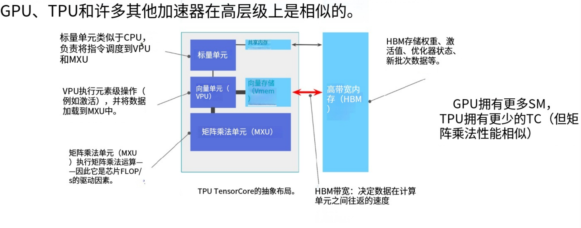
TPU internally has Tensor Cores, corresponding to GPU's SMs — independent atomic units. TPU's internal structure contains: scalar unit (control logic, similar to CPU), vector unit (element-wise vector operations), MXU (Matrix Multiply Unit): occupies the largest chip area, dedicated to matrix multiplication, vector memory + SM memory (on-chip high-speed storage), HBM (off-chip high-bandwidth memory).
The essential difference between TPU and GPU: TPU only optimizes matrix multiplication, doesn't attempt general-purpose computation — simpler architecture. TPU has no Warps, only Blocks — just a balance between matrix multiplication and non-matrix-multiplication.
What we call Tensor Cores can be analogized to SMs (Streaming Multiprocessors). Each Tensor Core is an independent atomic unit capable of processing data. It contains a scalar unit (essentially a control unit) that can also execute arbitrary operations similar to CPU; vector units suitable for element-wise vector operations; the chip's largest portion is dedicated MXU hardware for matrix multiplication; along with extremely fast vector memory and SM memory (all on-chip / Tensor Core memory).
Additionally, there is high-bandwidth memory located off-chip. Its similarity to SM lies in: external slow memory, internal fast memory; and dedicated matrix multiplication hardware. The core structure is highly consistent, with differences in accelerator interconnect methods. Tensor Cores are very simple in some respects because they are optimized exclusively for matrix multiplication. Unlike GPU, Tensor Cores attempt no tasks beyond matrix operations, hence an architecturally simpler design, though conceptually analogous.
Tensor Cores are called tensor processors because they can process tensors of arbitrary dimensions. They can indeed operate on arbitrary tensors and perform indexing operations. The core operation executed by MXU is matrix multiplication, so it always resembles batch matrix multiplication operations on tensors. It processes tensors, but the actual execution is always matrix multiplication, not more complex tensor operations.
GPU's success lies in excellent scalability. Simply increasing SM count boosts compute power without worrying about heat dissipation from higher clock frequencies. Programming-wise, CUDA appears complex but isn't actually frightening due to its programming model design — within each SM, threads execute the same instruction on different data, a concept that's easy to understand. Especially for simple matrix operations, this clean model shines. Furthermore, threads are very lightweight, can pause or start at any time, enabling GPU to achieve extremely high utilization within each SM.
6.5 Performance Scaling Trends
6.5.1 We Want Matrix Operations Fast and Good
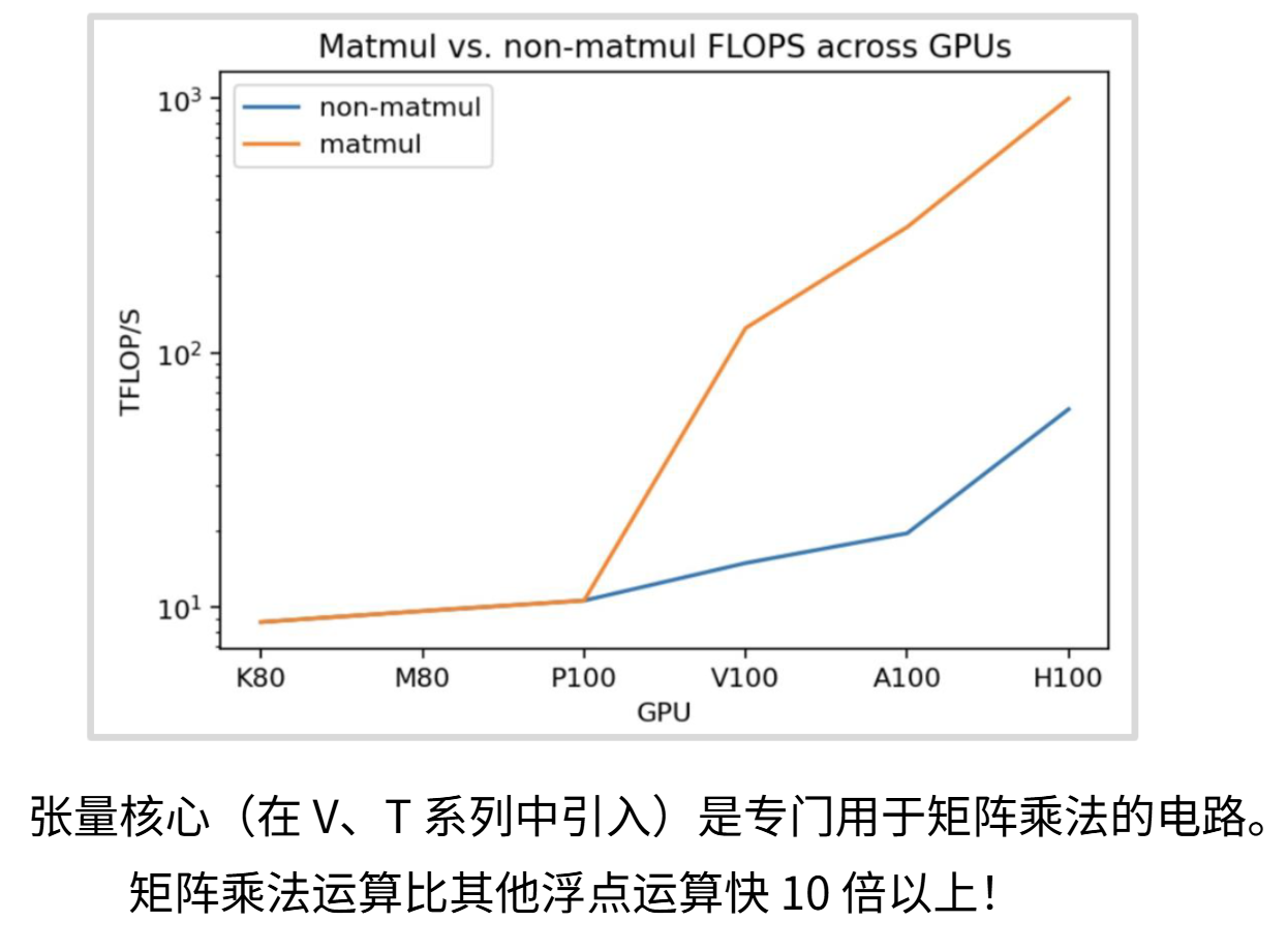
From the figure above, we can see that starting from P100 in the GPU lineage, blue non-matrix operations and yellow matrix operations began diverging dramatically, showing enormous difference. The primary reason: GPU vendors deliberately added Tensor Cores — circuits specifically optimized for matrix multiplication.
6.5.2 Compute and Memory Scaling Imbalance
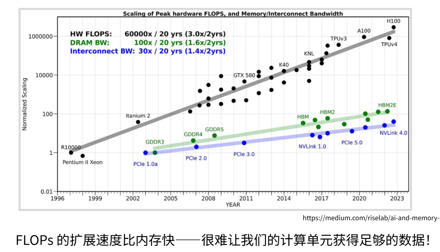
From 1980-2000, Dennard Scaling held — transistors shrank, frequency rose, power decreased. But the current situation: single-thread performance plateaued after 2000, unable to rely on frequency improvements. Modern scaling approach is parallel scaling (increasing SM count). From K20 to H100, integer compute performance shows super-exponential growth (10,000-100,000× improvement).
But the core contradiction remains unresolved — memory scaling is far slower than compute scaling. Compute performance (gray line): 100,000× improvement; memory bandwidth (green line): approximately 100× improvement (GDDR→HBM2e); interconnect bandwidth (blue line): slowest growth.
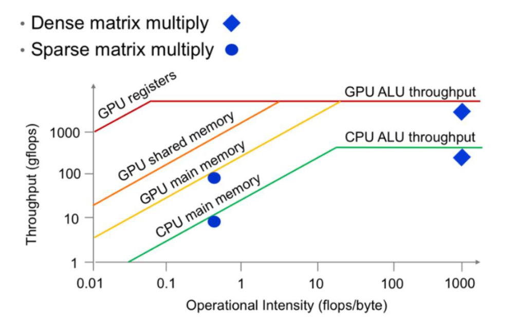
This is a Roofline Model. The horizontal axis is Operational Intensity, representing the ratio of computation to data movement. When operational intensity is high, the compute device is doing lots of computation with relatively little data movement; when low, data movement dominates. The vertical axis is Throughput, representing how many floating-point operations the compute device can complete per second.
Different colored lines represent different memory structures:
- GPU registers (red line): Provides the highest throughput because register access is very fast, but capacity is limited.
- GPU shared memory (orange line): Second fastest, suitable for scenarios requiring data sharing among multiple threads.
- GPU main memory (yellow line): Slower but larger capacity, suitable for storing large amounts of data.
- CPU main memory (green line): Even slower, because CPU memory access speed is typically lower than GPU memory.
The roofs they hit (memory walls):
- GPU ALU throughput: Represents the GPU's Arithmetic Logic Unit's maximum throughput under ideal conditions.
- CPU ALU throughput: Represents the CPU's Arithmetic Logic Unit's maximum throughput under ideal conditions.
The chart shows that as operational intensity increases, throughput across different memory levels also increases until reaching a certain ceiling. This ceiling is determined by the bandwidth and latency characteristics of the memory hierarchy. For example, GPU registers, due to their high-speed access characteristics, can achieve high throughput at low operational intensity but have limited capacity. CPU main memory, due to slower access speed, has relatively low throughput even at high operational intensity.
Now we can see the future trend: the memory wall problem will continue worsening. Algorithm design must be memory-centric — not a single bit of precious memory can be wasted. We must understand GPU memory structure changes to keep computation fast without wasting memory.
When examining throughput or utilization, two states exist. The left region of the curve is memory-bound, while the right region is compute-bound. From one perspective, the right region means compute units are fully loaded — all matrix multiplication units constantly computing; the diagonal region has some memory bottleneck, where compute capability is limited by computational intensity (FLOPs per byte). Therefore, we need to avoid the left memory-bound region and strive to be in the right region for full compute unit utilization. In summary: the key is to avoid unnecessary memory access, minimizing access frequency to slow global memory.
6.6 Performance Optimization Techniques
6.6.1 Avoid Serial Execution (Branch Divergence)
Below is a simple branch prediction example:
// Code example
if (x < 4) {
    A; // x < 4 executes
    B;
} else {
    X;  // x >= 4 executes
    Y;
}
Z; // Executes regardless of x
GPU uses SIMT (Single Instruction, Multiple Threads) execution architecture — all threads within the same Warp must synchronously execute the same instruction (only operating on different data). In modern GPUs, a Warp typically contains 32 threads (NVIDIA) or 64 threads (AMD).
When threads within a Warp encounter a conditional branch, if some threads satisfy x < 4 taking the if path while others satisfy x >= 4 taking the else path, Branch Divergence occurs. At this point, GPU uses mask-based serialization: first executes the if branch, with threads on the else path temporarily masked; after if completes, executes the else branch, with if threads masked. Both paths' instructions are executed, just with only some threads active each time. This causes the Warp's execution time to approximately equal the sum of both paths' duration — compute resource utilization drops.
Therefore, the core optimization principle is: avoid thread divergence within the same Warp — minimize conditional branches. If all threads in a Warp take the same path (e.g., all thread x values < 4), branch overhead is nearly zero. Furthermore, divergence not only extends execution time but may also disrupt memory access coalescing, further reducing bandwidth efficiency.
6.6.2 Low-Precision Accelerates Performance
Precision improves GPU speed by trading precision for faster computation and "much more saved" bandwidth. Behind this is the triple optimization of simplified hardware circuits, reduced data storage, and dedicated acceleration units. Most obviously: when the bit count of all elements like computation data and weights decreases, the amount of bits needing movement drops dramatically. Even accessing these bits from global memory, the impact becomes negligible.
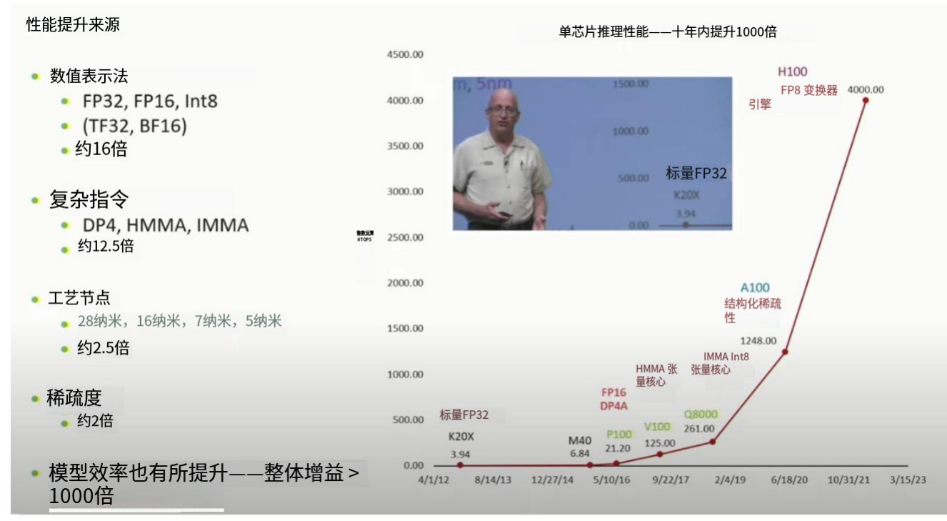
I. Common Low-Precision Formats
| Precision | Bits | Range | Typical Scenario | Speedup |
|---|---|---|---|---|
| FP32 | 32-bit | 3.4×10³⁸ | Traditional training, precision-sensitive | Baseline |
| FP16 | 16-bit | 6.5×10⁴ | General training/inference | 2-4× |
| BF16 | 16-bit | 3.8×10³⁸ | AI training preferred | 2-4× |
| TF32 | 19-bit | 3.4×10³⁸ | A100+ default format | 5-10× |
| INT8 | 8-bit | 2⁸ ≈ 256 | Quantized inference | 8-16× |
| INT4 | 4-bit | 2⁴ = 16 | Extreme inference | 16-32× |
| FP8 | 8-bit | Dynamic range | Hopper/Blackwell | 10-20× |
II. Low-Precision Speedup Mechanism 1: Hardware Factors
We know floating-point unit complexity is proportional to the square of bit width. That is, the larger the bit count, the larger and more complex the floating-point unit. FP16 multiplier transistor count is only 1/4 of FP32. This means more low-precision floating-point units can fit in the same area. More compute units mean stronger compute capability.
FP16 data occupies only half the register space of FP32 — the same 256KB register file can store twice the data. Meanwhile, 16-bit data bus bandwidth requirement is halved — the same bandwidth can transmit twice the data. And FP16 multiplier latency is lower, allowing higher frequency.
III. Low-Precision Speedup Mechanism 2: Memory Bandwidth Savings (50% Data Reduction)
We know that at lower precision, model files with the same parameter count occupy less memory than at higher precision. For example, GPT-3 175B parameters: FP32 = 700GB; BF16 = 350GB; Activations: per-layer activation cache, FP32 = 16GB; FP16 = 8GB; Gradients: backpropagation gradients, FP32 = 16GB; FP16 = 8GB. Clearly, training memory at low precision is much lower than at high precision.
Simple bandwidth calculation: assuming HBM2e bandwidth 2TB/s, FP32 transmits 50 billion parameters per second; BF16 transmits 100 billion parameters per second (doubled).
So at low precision: weight loading time reduces multiplicatively; cache hit rate improves (same cache capacity, more data stored); VRAM can accommodate larger models (350GB LLaMA-65B can run on 80GB VRAM with BF16).
IV. Low-Precision Speedup Mechanism 3: Tensor Core Dedicated Acceleration
Tensor Core is NVIDIA's dedicated circuit designed for low-precision matrix multiplication — not a scaled-down FP32, but a reconstructed matrix engine.
Ampere Architecture Tensor Core Performance:
| Precision | Peak Compute | Relative to FP32 CUDA Core |
|---|---|---|
| FP32 | 19.5 TFLOPS | 1× (baseline) |
| TF32 | 156 TFLOPS | 8× |
| FP16 | 312 TFLOPS | 16× |
| BF16 | 312 TFLOPS | 16× |
| INT8 | 624 TOPS | 32× |
Acceleration principles:
Systolic Array: Data flows through the array; each unit completes 1 multiply-add per cycle; 32×32 array completes 1024 operations per cycle. Weight Stationary: Matrix weights preloaded into array registers, reducing data movement. Accumulator Optimization: FP32 accumulator ensures precision; inputs/outputs use low precision.
V. Speedup Mechanism 4: Parallelism Boost (Same Chip Area, Doubled Compute Units)
Chip area optimization: as mentioned earlier, higher-precision compute units are more complex. 1 FP32 CUDA Core area ≈ 0.1 mm²; 1 FP16 CUDA Core area ≈ 0.05 mm² (50% saved); 1 INT8 CUDA Core area ≈ 0.025 mm² (75% saved).
Unique architecture design: in A100's SM, Tensor Cores reuse the register file. FP32 mode: 64 CUDA Cores active, 64 FMA per cycle; FP16 mode: 64 CUDA Cores + 4 Tensor Cores active, 64 FMA + 1024 matrix operations per cycle.
Same chip area, low precision can integrate 4× compute units, achieving 4× throughput.
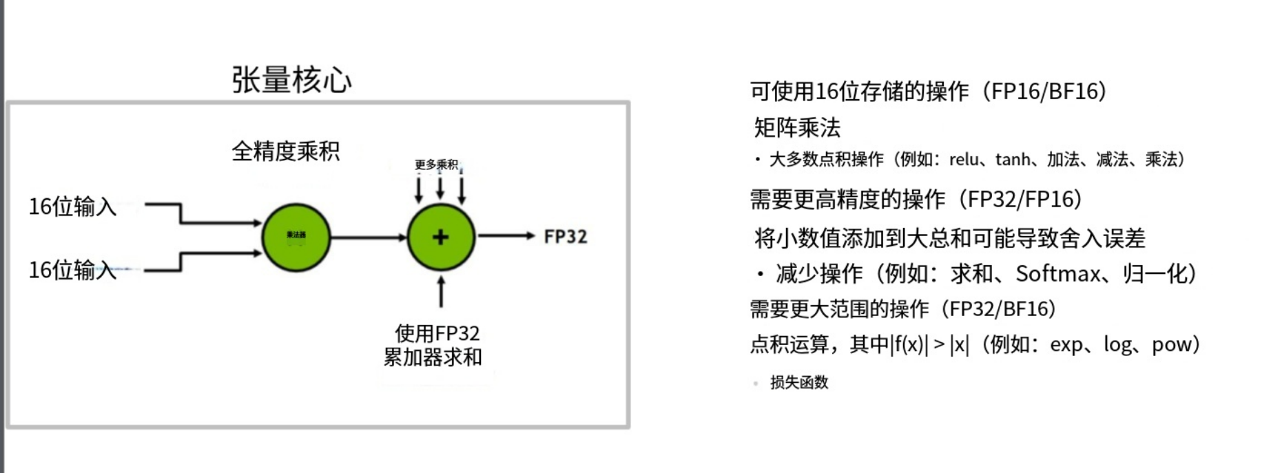
The key point: not all network components and training algorithms are suitable for low-precision processing. Taking matrix multiplication as an example: mixed-precision matrix multiplication typically sets inputs to 16-bit low precision, but multiplication maintains full 32-bit precision. This is because during partial sum accumulation, intermediate computation needs high-precision guarantee, hence FP32 accumulators are used. Tensor Cores ultimately output FP32 results, which can be reduced back to 16-bit as needed. Thus, input data can use 16-bit storage, but accumulation operations need 32-bit precision; certain operations (like exponential functions) need larger dynamic range and may suit BF16 format. Ensuring model stability during low-precision training requires extensive careful engineering optimization. But when achievable, when memory is the bottleneck, switching from 32-bit to 16-bit directly doubles throughput.
6.6.3 Operator Fusion
Operator fusion achieves 2-5× speedup by eliminating intermediate result memory reads/writes and reducing Kernel launch overhead.
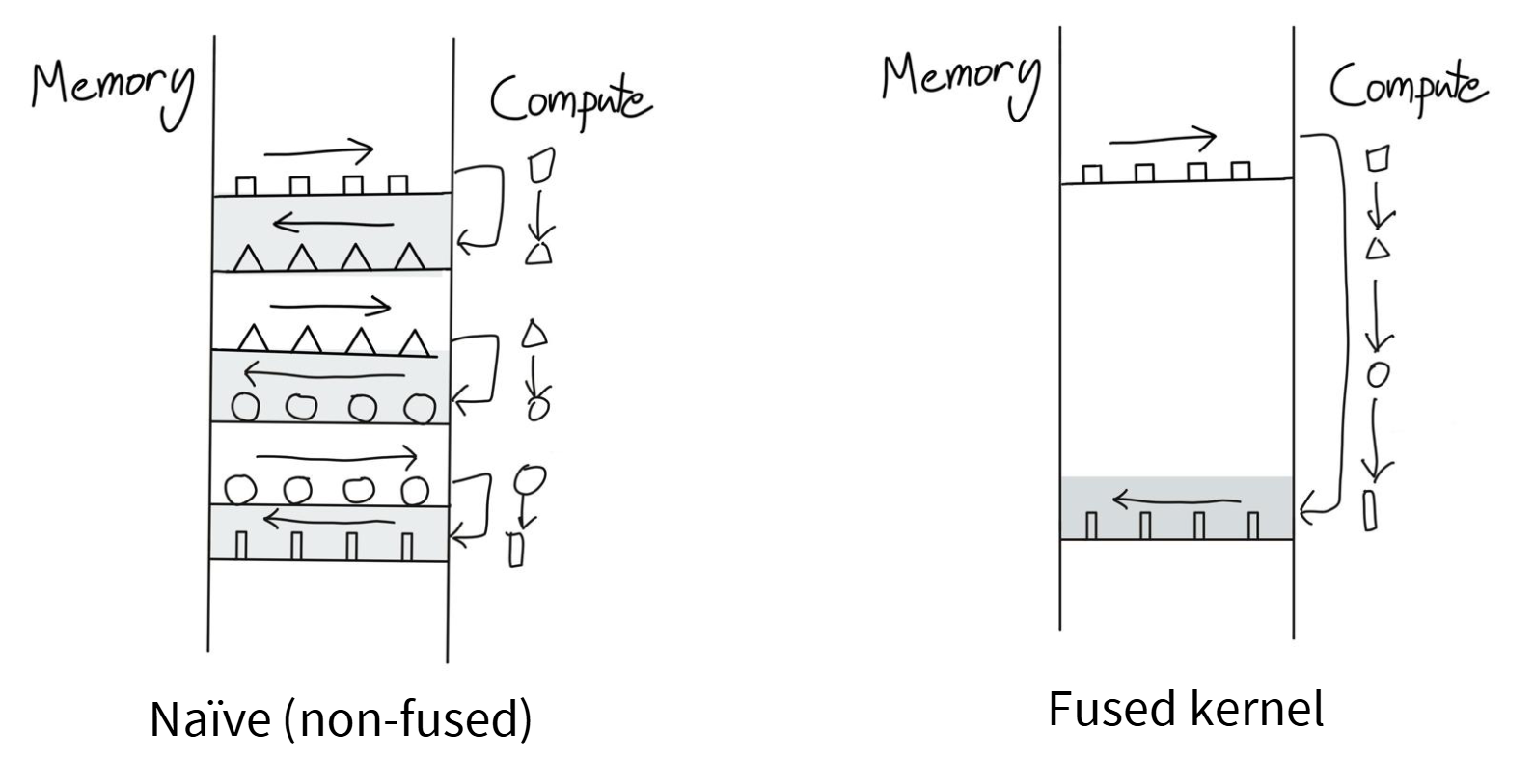
We can view GPU compute units as a factory: input square parts, output triangular parts. If compute capability increases but memory transfer bandwidth is limited (like a conveyor belt with fixed capacity), newly added factory equipment cannot be fully utilized — overall performance remains constrained by memory-to-compute transfer rate.
Imagine the left side of the left diagram is the memory region, and the right side is the compute unit. When performing operations, we start with square data, move it from memory to compute unit, perform operations to transform it into a triangle, then move the triangle back to memory. Then we discover we need those triangle data again, so we feed them back into the compute unit, triangle becomes circle, and so on. Data shuttles back and forth between compute unit and memory. If we directly do simple operations on GPU and immediately write results back to global memory, this pattern emerges. Counting round-trips for a single data block, this approach is extremely inefficient, generating enormous memory overhead.
Now observe the right-side computation flow: we discover these operations have no dependencies, so we directly transform square → triangle → circle → rectangle, then transfer back to memory. We keep all data continuously resident in the compute unit.
This is essentially the mental model of kernel fusion. When a series of operations needs to process the same data sequentially, rather than writing intermediate results back to storage each time, it's better to complete all operations within a single compute unit as much as possible, only transferring to memory when it must be transmitted. This is the core idea of kernel fusion.
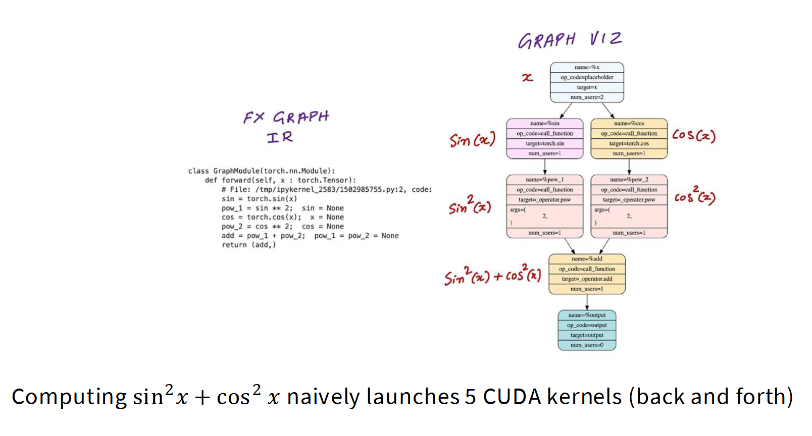
Suppose we write a neural network module: input
But we realize these five operations have no complex dependencies, need only small amounts of memory, and can be completely fused into a single operation, completing all processing on a single GPU thread without writing data back to global memory.
In essence, operator fusion merges multiple consecutive operations into a single CUDA kernel, avoiding intermediate results being written to global memory.
6.6.4 Recomputation (Gradient Checkpointing)
The core idea of recomputation is using extra computation to avoid memory access.
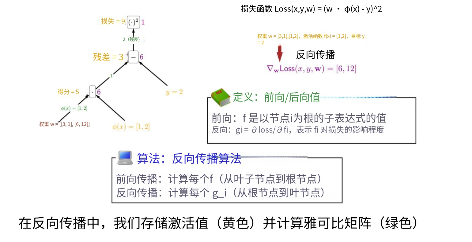
We take the bottom-layer input data (yellow nodes), then propagate activations upward. These are also the yellow values on the tree. Then we backward-compute Jacobians. These are the green values on the edges. To compute gradients, we backpropagate — requiring multiplication operations. We combine Jacobians with activations, backpropagating gradients. Think carefully: those yellow values after forward propagation must be stored. After being stored, they need to be fetched from the global memory where we placed them and fed into the compute unit.
Mechanistically, this process is inevitable. But it can lead to massive memory I/O operations. However, this can be avoided.
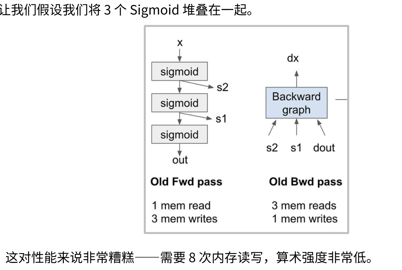
Suppose we stack three
And the core idea of recomputation is: don't store those activations, don't put them in memory — instead, dynamically recompute them during backpropagation. In the new forward propagation, don't store S1 and S2: input
Overall, this recomputation doesn't store S1 and S2 but recomputes them during backpropagation. This is a trade-off between computation time cost and memory read/write time cost — recomputation suits scenarios where computation cost is less than read/write cost.
By recomputing S1, S2, and output values in real-time in local memory, we avoid global memory read operations and finally need only one memory write for dx. While completing the same computation, we now need only 5/8 of the memory accesses. The cost is having to recompute those three sigmoid functions. But if compute units were already idle due to memory bottlenecks, this is very worthwhile — using surplus compute power to buy scarce memory bandwidth.
6.6.5 Memory Coalescing
The slow memory in GPU (i.e., global memory/DRAM) is actually extremely slow. To improve speed, hardware-level specific optimizations are performed.
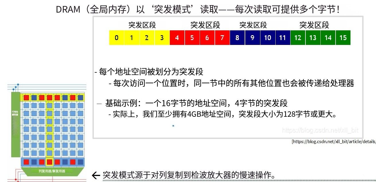
One DRAM hardware optimization: when reading a memory value, what you actually get is not just the target value, but an entire block of memory data — this is called burst mode. Suppose you read the first value of a large memory block; memory returns not just 0, but simultaneously returns all four values 0, 1, 2, 3.
Each address space is divided into burst segments; the system directly returns the entire burst segment rather than just the target data. When addressing memory, data transfer to the amplifier is the most time-consuming step. The burst segment's role is: once this step is complete, you can freely obtain large amounts of byte data. Burst segment design is precisely for optimizing the time-consuming data migration process. If memory access patterns are appropriate, memory access can be significantly accelerated. For example, to read an entire data block, random access requires as many operations as the query length; but if you first read the first value, you immediately get the entire burst segment; then read the 4th value, immediately getting the second burst segment. Through carefully designed memory access strategies, extracting only needed data from each burst segment, theoretically achieving 4× throughput — this is memory coalescing.
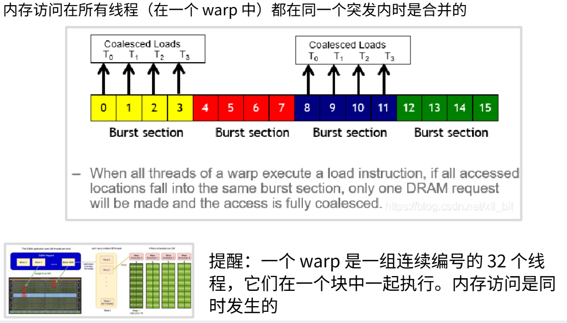
When all threads in a Warp are within the same burst segment, intelligent hardware and programming models aggregate these queries — no longer individually querying 0,1,2,3, but through a single query of 0, simultaneously reading all four values from burst-mode DRAM. Note that a Warp contains 32 ordered threads — these threads' memory accesses occur synchronously. Through optimization, all 4 bytes of data can be obtained at once, boosting memory throughput by 4×.
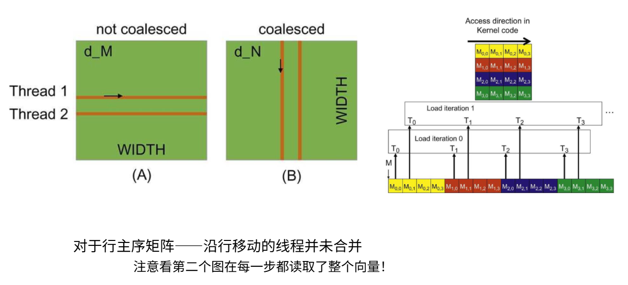
Taking matrix multiplication as an example, suppose there are two matrix access patterns: row-major traversal (each thread processes one row) or column-major traversal (each thread processes one column). In practice, the left-side column-major traversal pattern is very slow because memory access cannot be coalesced; while the right-side row-major traversal has threads accessing consecutive memory addresses, enabling memory coalescing.
The right side shows a matrix and its position in memory. Taking matrix multiplication as an example, assuming the matrix is stored in row-major order. Consider two thread access patterns:
1) Each thread handles one entire row of the matrix; 2) Each thread handles one entire column of the matrix.
When each thread handles one row, threads within the same Warp access memory addresses far apart from each other — this access pattern cannot achieve memory coalescing, resulting in low memory bandwidth utilization and poor performance. Conversely, when each thread handles one column and accesses different column elements of the same row at the same time step, threads within the Warp access consecutive memory addresses, achieving full memory coalescing and significantly improving access efficiency.
From a memory layout perspective, if a group of threads accesses consecutive elements of the same row in a matrix from left to right, these accesses all fall within the same or adjacent memory burst segments, requiring only one or a few memory transactions to complete data loading. But if thread access addresses are scattered across multiple non-consecutive memory burst segments, each access may trigger an independent memory transaction, causing actual memory access speed to fall far below theoretical bandwidth.
This difference in memory access ordering is a very low-level optimization detail, but is critically important in GPU programs; if traversal order is improperly designed, performance often degrades by orders of magnitude.
6.6.6 Tiling
The core idea of tiling is reducing global memory access volume by grouping memory accesses.
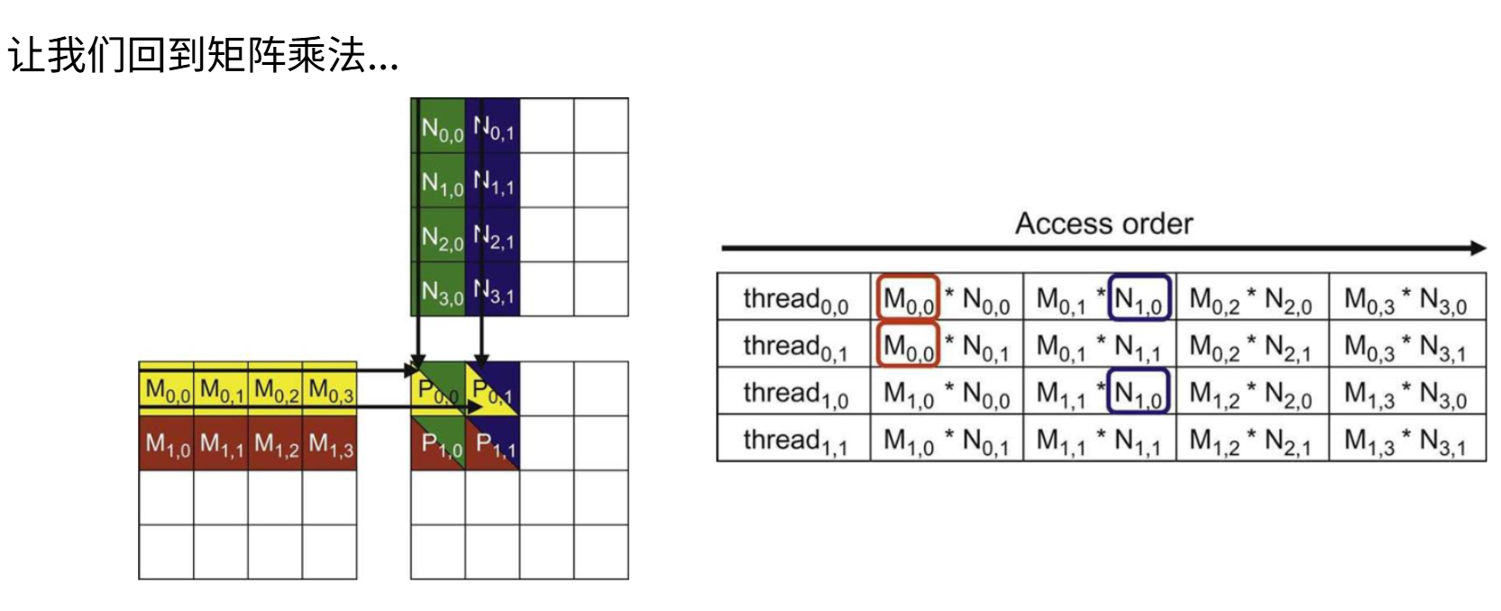
Explaining through the matrix multiplication example: the original matrix multiplication algorithm has a serious problem. Starting from this simple matrix multiplication algorithm: the left side is the
Here memory access is non-coalesced — the row matrix's access order is non-consecutive and has repeated memory accesses. For example,
The question is whether we can avoid excessive global memory reads/writes. The ideal approach: spend some time loading data blocks from global memory into fast shared memory, complete substantial computation in shared memory, then process the next data block. This minimizes global memory access.
化.png)
In matrix multiplication, we divide both
Another advantage: since we load complete data tiles, we can traverse these sub-matrices in arbitrary order (e.g., column-major or row-major), thereby achieving memory access coalescing when loading data tiles from global memory into shared memory. The tiling access strategy brings comprehensive performance improvements.
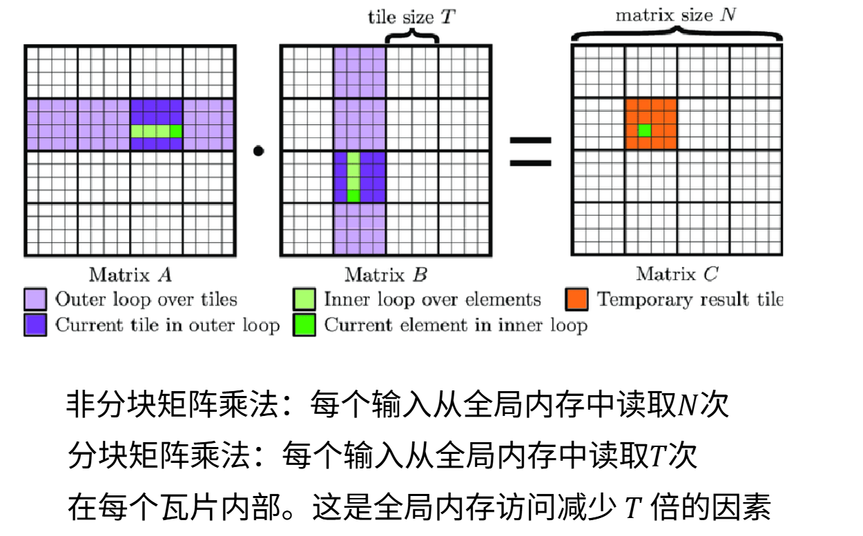
Now we can perform mathematical analysis of tiled computation. Suppose matrices
分块的复杂性.png)
Tiling strategy is very complex — this is one root cause of confusing GPU and matrix multiplication performance behavior. Suppose we use a regular tile size of 128 — when processing a complete 256-size matrix, it works well, with 2×2 tile data loading smoothly. But suppose we use a tile size of 257 in the column direction — then six tiles are needed to cover this matrix, and the two right-side tiles contain no data. The problem is each tile is assigned to a Streaming Multiprocessor (SM) — each tile corresponds to a thread block, threads execute operations within their respective tiles. So those two right-side tiles perform almost no computation, and the corresponding SMs remain essentially idle.
If encountering computation bottlenecks, we want to distribute load more evenly across SMs, so we must optimize tile sizes to avoid such situations. But determining tile size involves many complex factors. Memory access coalescing must be achieved without exceeding shared memory capacity, so tiles can't be too large; matrix dimensions must be partitioned, ideally evenly or near-evenly divisible, avoiding extremely low SM utilization.
Another very deep and detailed complex issue is the interaction between tile partitioning and burst transfer segments. Suppose the matrix layout is very regular — each burst transfer segment perfectly aligns with tiles. Reading this tile only requires fetching four different burst transfer segments to load the entire tile. But if we add one element at the end, the matrix layout causes burst transfer segment misalignment.
For instance, in the figure above, when loading a tile, the first row can still be loaded as one complete burst transfer segment, but the second row is split across two different burst transfer segments, requiring two reads to obtain, and so on. Simply because one extra element at the end causes memory access volume to double — this is burst transfer segments becoming misaligned with the layout. Essentially, if tile or matrix dimensions are not integer multiples of burst transfer segments, such row-to-burst-segment misalignment easily occurs, causing memory access volume to double. The solution is using padding to make matrix dimensions regular, realigning burst transfer segments with tile sizes. Although these are very low-level concerns, fully exploiting matrix multiplication performance requires considering these details. Ignoring them may lead to performance traps during actual execution.
6.7 Flash Attention
Figure 6.24 FlashAttention V1 Schematic
Standard Transformer Attention has
FlashAttention does not change Attention's asymptotic computational complexity (FLOPs remain
FlashAttention is mathematically equivalent to standard attention (except for floating-point error) — it's exact rearrangement, not approximate computation. Try running FlashAttention.ipynb to compare FlashAttention and standard Attention computation results.
Figure 6.25 Left: Forward+Backward runtime; Right: Attention memory usage.
From Figure 6.25's analysis, although different Attention implementations have similar runtimes, FlashAttention's memory footprint is clearly lower — roughly half that of other implementations. Therefore, in long-sequence scenarios, FlashAttention has better scalability and higher resource utilization efficiency.
6.7.1 FlashAttention V1 Computation Principle
Where Q, K, V are all
# Initialization
m_i = -inf
l_i = 0
O_i = 0
for each Q block i:
    load Q_i
    m_i = -inf
    l_i = 0
    O_i = 0

    for each K,V block j:
        if causal and j > i:
            continue

        load K_j, V_j
        S_{ij} = Q_i @ K_j^T      # (B_r, B_c)

        if causal and i == j:
            apply mask to S_{ij}

        # softmax accumulation → reduction
        update m_i, l_i, O_i (online softmax)

    write O_i to HBM
Why does FlashAttention V1 need tiling (tile/block)?
In GPU, the main bottleneck of Attention computation is cache (SRAM) capacity and compute bandwidth. Directly computing
generates an intermediate matrix — when is large, it cannot fit entirely in cache, and frequent HBM access increases cache pressure. FlashAttention's core idea is: through tiled computation, reduce global memory access, improve cache utilization, and ensure computational efficiency and numerical stability. The specific approach: process small tiles that fit in SRAM while simultaneously performing softmax accumulation, thereby大幅 reducing global memory access pressure.
Concrete example:
- Suppose Q, K shapes are
. - Partition Q into 8 tiles by rows, each tile
; partition into 8 tiles by columns, each tile . - Each time only compute a
sub-matrix in SRAM and accumulate results, until completing the entire and computation.
6.7.2 Online Softmax
Online softmax is mathematically completely equivalent to standard softmax — both require global normalization. The difference is that online softmax uses streaming computation, dynamically maintaining the current maximum value and normalization factor (exponential sum) during traversal, thus not needing to store complete intermediate results. This streaming property enables natural integration with tiled computation. In FlashAttention, Attention scores are computed tile by tile, with maximum values and normalization factors continuously updated across tiles to achieve cross-tile global normalization.
Online softmax's detailed role in FlashAttention V1 computation:
m_{ij} = rowmax(S_{ij})
m_new = max(m_i, m_{ij})

l_i = exp(m_i - m_new) * l_i
  + sum(exp(S_ij - m_new), axis=1)

O_i = exp(m_i - m_new) * O_i
  + exp(S_{ij} - m_new) @ V_j

m_i = m_new
O_i = O_i / l_i
Thus, online softmax becomes the key component enabling FlashAttention V1 to complete exact Attention computation without explicitly constructing the entire attention matrix.
6.7.3 FlashAttention V2: Tensor Core-Oriented Parallel Optimization
FlashAttention V1 solved the attention computation memory bottleneck through tiling and online softmax, but its loop order and parallel strategy did not fully exploit the peak throughput of matrix multiplication (Tensor Core) in modern GPUs (especially A100 and later architectures). V2, while maintaining V1's core ideas, deeply restructured the algorithm to achieve more efficient parallelism and lower non-matrix-multiplication overhead.
FlashAttention V2's Core Improvement: Tiled Parallelization of Q
In FlashAttention V1, computation uses an outer loop over IO efficiency — the problem is: this process involves cross-tile online normalization and rescaling operations (max, exp, rescale) forming a data dependency chain, making execution manifest as alternating patterns of matmul → reduction (normalization) & scalar update → matmul → reduction & scalar update.... These non-matmul operations reduce Tensor Core utilization and limit operator fusion and parallel scheduling efficiency.
FlashAttention V2 does not change the basic data loading order of data dependency chain:
- Changes the original "one
corresponds to one thread block serially scanning all " approach to partitioning the same across the dimension, processed in parallel by multiple thread blocks (split-KV parallelism); - Preserves online softmax's mathematical form, but through tiled parallel computation + cross-thread-block reduction, transforms the original "serial dependency processing" along the
dimension into parallel computation + end-stage reduction, thereby significantly improving parallelism and hardware utilization.
for each Q block i in parallel:              # V2's core: Q dimension parallel
    load Q_i into SRAM

    # Initialize
    m_i = -inf
    l_i = 0
    O_i = 0

    for each K,V block j:
        load K_j, V_j into SRAM

        S_ij = Q_i @ K_j^T                  # Tensor Core
        m_ij = rowmax(S_ij)
        m_new = max(m_i, m_ij)

        # Rescale old accumulation
        alpha = exp(m_i - m_new)
        P_ij = exp(S_ij - m_new[:, None])
        l_ij = rowsum(P_ij)

        # Update normalization factor
        l_new = alpha * l_i + l_ij

        # Update output (core optimization point), online softmax accumulation
        O_i = (alpha[:, None] * O_i) + (P_ij @ V_j)
        m_i = m_new
        l_i = l_new

    # End-stage reduction
    O_i = O_i / l_i[:, None]
    write O_i back to HBM
Reasons for V1 → V2 performance improvement:
(1). Reduce non-matrix computation interference with execution (not reduce its total amount)
In V1, every
(2). V2 does not reduce the mathematical count of these operations (still
It transforms the serial dependency along the
(3). Improved Tensor Core utilization (from scheduling and parallel restructuring, not "batch submission")
- In V1, due to online softmax's per-tile dependency, matmul and scalar updates alternate execution, limiting Tensor Core's sustained working capability;
- V2, through increased parallel thread blocks (especially split-KV), allows more matmuls to proceed simultaneously across different SMs, thereby improving Tensor Core's overall occupancy.
Notably, SM overall occupancy is not equivalent to its compute unit utilization. Even if thread blocks fully fill SMs, if synchronization waits exist between data loading and computation, Tensor Cores and other execution units may still idle. FlashAttention V3 was proposed against this background, introducing asynchronous execution and pipeline mechanisms to further improve computation-data-transfer overlap, reducing hardware idle time.
Thus, the essence of V2's improvement is: more parallel matmul + less serial dependency, not "batch-submitted" matmul within a single thread.
One-sentence comparison of V1 and V2 — FlashAttention V2's essence is not reducing FLOPs, but rewriting "online softmax's temporal serial dependency" into "spatial parallelism."
Tile Size and Hardware Adaptation
V2 made fine adjustments to tile sizes to match GPU SRAM capacity and register resources. Taking A100 as an example, each SM has 192KB shared memory. V2 selects
Performance
- Speedup: On A100, for sequence lengths 512-16k, V2 averages 1.7~2.0× acceleration vs V1, and 8~10× vs PyTorch standard implementation.
- Memory footprint: Consistent with V1, still
, but maximum supported sequence length expands due to computational efficiency improvement (single 40GB A100 can stably train 32k length). - Hardware adaptability: V2's optimization strategy is equally effective for Ampere and subsequent architectures (like H100), laying the efficient parallelism foundation for the next version (V3).
FlashAttention V2, by improving parallelism in the sequence dimension and optimizing computation scheduling, significantly boosts Tensor Core utilization while maintaining V1's IO-awareness特性, thereby pushing attention computation's overall throughput to higher levels. This improvement makes long-context Transformer training and inference more efficient in single-card or resource-constrained environments, becoming an important optimization component in modern high-performance Transformer systems and adopted or referenced by various LLM engineering implementations including Llama 2, GPT-4, etc.
6.7.4 FlashAttention V3: Asynchronous and Low-Precision Optimization
FlashAttention V2 approached Tensor Core's theoretical limits on A100 and other Ampere-architecture GPUs, but H100 (Hopper) architecture introduced revolutionary new features: asynchronous execution model (supporting full overlap of computation and data movement), WGMMA (Warpgroup Matrix Multiply-Accumulate) instruction, and native FP8 support. V3 is the product of deep optimization targeting these hardware features, aiming to make attention computation achieve near-peak throughput on H100 and fully leverage the compute dividend of low-precision formats.
FlashAttention V3's Core Improvement: Asynchronous WGMMA Pipeline
FlashAttention V3 is not built on changes to the "Q outer, K/V inner" loop order, but rather, building on V2's existing parallel and reduction framework, reconstructs the underlying execution mechanism. Its core improvement is introducing NVIDIA Hopper's (e.g., H100) asynchronous computation capability, organizing the computation flow as a producer-consumer pipeline.
The core idea leverages Hopper architecture's asynchronous instructions (such as TMA data movement and WGMMA matrix multiplication) to achieve:
- Decoupling data loading (global → shared memory) from Tensor Core;
- Cross-warp-group pipeline parallel execution: while computing one block, prefetch data for the next block.
Thus significantly reducing SM idle cycles caused by data waiting, making GPU execution cycles closer to ideal sustained computation state.
# Initialize double buffer
buffer_K[2], buffer_V[2]

for each Q block i:
    load Q_i

    async_load(buffer_K[0], buffer_V[0])

    for j in range(num_blocks):

        curr = j % 2
        next = (j + 1) % 2

        # Producer, preload next block
        if j + 1 < num_blocks:
            async_load(buffer_K[next], buffer_V[next])

        # Consumer, compute using current buffer
        S_ij = wgmma(Q_i, buffer_K[curr])

        update m_i, l_i   # softmax reduce

        O_i += wgmma(P_ij, buffer_V[curr])

        # Only sync when necessary (avoid stall)
        wait_for(buffer_K[next])

    write O_i
WGMMA (Warpgroup Matrix Multiply-Accumulate) is a new instruction type introduced by H100. It organizes a group of warps (32 threads) into a warpgroup (4 warps, 128 threads total) and directly supports asynchronous execution at the hardware level. V3 splits
H100's FP8 Low-Precision Support and Mixed Precision
H100's 4th-gen Tensor Core has theoretical FP8 throughput twice that of FP16 (e.g., H100 SXM's FP8 peak is approximately 1979 TFLOPS vs FP16's 989 TFLOPS). V3 natively supports FP8 input, but must solve numerical stability problems in attention computation because softmax is precision-sensitive.
Therefore, V3 adopts a mixed precision strategy to boost performance:
Matrix multiplication
Additionally, V3 implements dynamic scaling factor management. Since FP8 has limited representable range (E4M3 approximately -448 to 448, E5M2 approximately -57344 to 57344), scaling factors must be determined based on input range before computing
Tile Layout and Register Optimization
H100's each SM has 256KB shared memory (larger than A100's 192KB), with more abundant register file as well. V3 readjusts tile sizes
More importantly, V3 finely controls register usage to avoid register spilling to local memory (L1 cache). By keeping intermediate statistics (
Performance: computational efficiency and speed, long-sequence capability all improved
- Computational efficiency: On H100 SXM using FP8, V3's TFLOPS utilization reaches 75%~80%, approaching theoretical peak. This means attention computation is almost no longer limited by memory bandwidth, but entirely computation-driven.
- Speedup: Compared to V2's FP16 implementation on H100, V3's FP8 version is approximately 1.5~2× faster; even at the same FP16 precision, V3's asynchronous optimization brings approximately 1.3× acceleration.
- Long-sequence capability: On sequences of 128k and even 1M length, V3 still maintains extremely high throughput, dramatically reducing training and inference costs for ultra-long-context models. A single H100 80GB card can stably train 256k-length models.
FlashAttention V3 is a paradigm of algorithm-hardware deep co-design. It decouples data loading and computation through asynchronous WGMMA pipeline, unleashes H100's low-precision compute power through FP8 mixed precision, and eliminates memory bottlenecks through fine tile layout and register optimization. This series of improvements makes attention computation no longer a barrier to Transformer long-context scaling, but a "high-performance component" that fully exploits hardware limits. V3's birth directly underpins the engineering implementation of current industrial 100k~1M context window LLMs.
Summary of FlashAttention development:
- V1 solved the IO bottleneck;
- V2 solved parallel scheduling and GPU utilization;
- V3 solved computation-memory-access overlap (SM work efficiency).
In one sentence: from "reducing memory bandwidth bottleneck" → "improving parallel scheduling and GPU utilization" → "achieving computation-memory-access overlap, keeping SMs always busy."
6.8 PagedAttention
Figure 6.26 Traditional KV Cache Distribution
In traditional KV Cache management, each request sequence is typically pre-allocated a logically contiguous cache space for storing its historically generated Key/Value states. However, since actual generation length is difficult to predict accurately, this static pre-allocation strategy causes memory utilization problems. When reserved space exceeds actual generation length, internal fragmentation occurs — allocated but unused memory space. Simultaneously, due to different requests having inconsistent lifecycles and varying release times, memory may contain many scattered free blocks. At this point, although total free capacity is sufficient, it cannot provide large enough contiguous cache blocks to satisfy new sequence allocation demands, producing external fragmentation.
Figure 6.27 Memory Footprint Analysis
The above fragmentation problems significantly reduce GPU High Bandwidth Memory (HBM) overall utilization efficiency. To mitigate this problem at the system level, based on operating system paging mechanisms, PagedAttention splits KV Cache into fixed-size pages and performs indirect address mapping through a page table, making logically contiguous KV storage no longer dependent on physically contiguous memory, thereby effectively reducing fragmentation and improving memory utilization.
6.8.1 PagedAttention Principle Analysis
In standard autoregressive (AR) inference, each newly generated token produces corresponding K and V, appended to the KV cache in chronological order. Logical order strictly corresponds to temporal order, while physical storage order depends on the specific implementation strategy. To ensure efficient GPU access and CUDA kernel memory access patterns (such as memory coalescing), traditional implementations typically organize KV cache as contiguous memory tensors and pre-allocate memory based on a preset maximum sequence length upper bound. However, since different requests have significantly different actual generation lengths, and GPU memory allocators struggle to support low-cost dynamic expansion and memory rearrangement, this maximum-length-based contiguous pre-allocation strategy easily produces internal and external fragmentation.
Let's illustrate the problems of contiguous physical memory in standard AR with an example. Suppose each request reserves contiguous KV cache physical space by maximum length of 2048 tokens:
If multiple requests of varying lengths exist simultaneously — say request A actually generates 128 tokens, request B 1024 tokens, request C 300 tokens:
Request A: 128 tokens
Request B: 1024 tokens
Request C: 300 tokens
Then the problems become apparent. Internal fragmentation manifests as: each request pre-occupies 2048-length contiguous physical space, but actual usage is far less, causing大量剩余空间 to be wasted (e.g., request C wastes over 1700 tokens of capacity). External fragmentation manifests as: many scattered small free blocks exist in memory, but no single contiguous region is available for use — this is particularly severe on GPU, causing fragmented free memory to be unallocatable to new requests.
vLLM's proposed PagedAttention precisely addresses the above problems — it transforms "static contiguous storage" into "dynamic paged management." The core idea is splitting KV cache into fixed-size blocks (Pages), e.g., each Page contains KV storage for 16 tokens. Through a Block Table, PagedAttention maps logically contiguous tokens' KV to physically possibly non-contiguous storage blocks, thereby maximizing memory space utilization. For example, three logically contiguous token segments (1–16, 17–32, 33–48) can be mapped through the page table to physical addresses Block7, Block2, and Block19 respectively — physically not adjacent.
Why does this eliminate the need for contiguous physical space? Because during Attention computation, the system reads KV block by block according to the page table: for each block processed, first look up the page table to find the corresponding physical block, then execute the read operation. As long as the page table maintains correct mapping relationships, even if physical addresses are non-contiguous, the read sequence logic remains correct. The entire flow can be simplified as:
for each block:
    Look up page table
    Find corresponding physical block
    Read
More importantly, this memory allocation process is on-demand and dynamic — as the request's actual generated token count grows, new pages are progressively allocated, rather than pre-reserving an entire block of space upfront.
PagedAttention transforms memory management from request-unit static reservation to token-unit dynamic allocation. Through physical address non-contiguous mapping, it completely solves the severe internal fragmentation problem in standard AR caused by reserving maximum length. Still using the 300-token request example, with each Page = 16 tokens:
- Required Page count:
, rounded up needs 19 Pages. - Actually allocated physical space:
tokens capacity. - Waste: only
tokens.
In contrast, standard AR reserving 2048 length wastes
A simple dining analogy helps understanding: Standard AR is like a "fixed-price full banquet" — regardless of how much you eat, you must reserve space for 2048 dishes. Eat 300 and leave — the remaining 1748 can only be discarded (memory forcibly occupied and unreusable). PagedAttention is an "on-demand buffet" — every 16 tokens is one plate; finish one plate before taking the next. Empty plates can immediately be given to other diners (memory dynamically reclaimable and reusable).
Thus, traditional AR's waste scale is
In summary, PagedAttention's working principle can be概括 as:
Virtual Address → Page Table → Physical AddressAt vLLM's source code level, its mapping logic can be expressed as:
Request ID + Token Offset → Logical Block Index → Block Table Lookup → Physical Memory Base → Offset Read6.8.2 FlashAttention vs. PagedAttention Comparison
Although PagedAttention and FlashAttention both appear committed to improving LLM inference performance, their optimization dimensions are fundamentally different.
FlashAttention primarily focuses on IO complexity within a single forward computation, belonging to operator-level micro-optimization. Through tiled computation (tiling) and online Softmax (log-sum-exp streaming) techniques, it avoids explicitly constructing the complete
PagedAttention focuses on memory management efficiency across the entire generation lifecycle, belonging to system-level macro-design. It does not change Attention's mathematical computation formula, but rather organizes KV Cache as fixed-size physical blocks (pages) and decouples logical order from physical order through a logical block table. This paging structure effectively mitigates memory fragmentation, supports dynamic batching and long-context inference, thereby improving memory utilization and concurrent throughput. PagedAttention solves the "store more efficiently" problem.
From several key dimensions, their differences become clearer. In optimization target, FlashAttention focuses on single forward-pass IO complexity, while PagedAttention focuses on memory management across the entire generation lifecycle. In time scale, the former is micro-level (operator-level) optimization, the latter is macro-level (system-level) optimization. In impact scope, FlashAttention acts on the attention kernel itself, while PagedAttention manages KV Cache lifecycle. Additionally, FlashAttention affects both training and inference, while PagedAttention is basically only applicable to inference; FlashAttention does not depend on decoder-only architecture, while PagedAttention has strong dependency on it.
In actual inference frameworks (such as vLLM), the two are typically used together to simultaneously optimize single-request latency and overall throughput. However, it's worth noting that PagedAttention introduces non-contiguous physical layout of KV cache through indirect addressing, which may break FlashAttention's assumptions about contiguous memory access and memory coalescing. Therefore, when used jointly, FlashAttention kernels typically need to adapt with page as the minimum streaming computation unit, or ensure block_size is close to tile_size to maintain shared memory utilization and memory access efficiency.
6.9 Domestic GPU Overview
Domestic GPU performance metrics are already quite impressive, especially in FP16 compute power needed for AI training — leading products have reached or approached international mainstream levels. More importantly, these compute capabilities have been validated in multiple real LLM training scenarios. While there's still distance to cover at the top-tier compute card level domestically, self-sufficiency is achievable at mid-to-high-end tiers. Currently, domestic GPUs have been developing primarily in the compute card direction, with relatively little investment in consumer graphics cards (for PCs or gaming).
6.9.1 Muxi Technologies
Muxi Technologies is an important force in the domestic GPU space, with 2025 revenue exceeding 1.6 billion RMB, transitioning from technology validation to scaled commercial deployment. The current主力 product is the XiYun C Series train-inference unified GPU, with next-generation products already in the pipeline.
In the XiYun product line, the XiYun C500 Series has achieved mass production. As the 2025主力 product, it targets NVIDIA A100, positioned for AI training and inference. The XiYun C600 Series has performance between A100 and H100, entering risk production at the end of 2025 with formal mass production expected in H1 2026. The next-generation flagship XiYun C700 Series directly targets NVIDIA H100 —立项 in April 2025, with tape-out planned for H2 2026.
6.9.2 Baidu Kunlun Chip
Baidu Kunlun Chip is one of the earliest players in the domestic AI chip space. Its predecessor was Baidu's internal Intelligent Chip and Architecture Department established in 2011 —可以说 it's a "veteran" of domestic AI chips. Unlike Huawei Ascend's "system architecture compensating for individual process nodes" approach and Biren's GPGPU focus, Kunlun's differentiated advantage lies in being refined through Baidu's real business scenarios, having been大规模 internally validated before entering the external market.
At the product level, the current主力 chip Kunlun Chip P800 was launched in 2024 and has been大规模 deployed. Using 7nm process, FP16 compute reaches 345 TFLOPS — 2.3× that of NVIDIA H20. In single-machine 8-card configuration, the DeepSeek一体机 delivers 2 PFLOPS (FP16) peak compute. Looking forward, Kunlun has planned multiple new products: Kunlun Chip M100 targets large-scale inference scenarios, emphasizing extreme cost-performance, launching in 2026; Kunlun Chip M300 targets ultra-large-scale multimodal model training and inference, planned for 2027. Meanwhile, Tianchi 256 Super Node and Tianchi 512 Super Node (supporting 256-card and 512-card interconnect respectively) will both debut in 2026, with the 512-card super node capable of completing trillion-parameter training on a single node, achieving over 50% overall performance improvement.
From market shipments, Kunlun has secured the #2 domestic position. According to IDC's 2024 China Accelerated Computing Chip Shipment Report, NVIDIA holds 70% share with over 1.9 million units, Huawei Ascend shipped 640K units ranking #1 domestically, Kunlun shipped 69K units ranking #2 domestically, followed by Tianshu Zhixin (38K units) and Cambricon (26K units).
Software Ecosystem and Commercial Deployment
In the software stack, Kunlun deeply supports mainstream AI frameworks. Chips come pre-installed with Baidu PaddlePaddle framework, simultaneously supporting TensorFlow, PyTorch seamless migration, and providing a "CUDA-like" programming environment, significantly reducing developer migration costs.
In cluster capability, Baidu AI Cloud this year lit up a 30,000-card cluster based on Kunlun P800, capable of simultaneously supporting multiple hundred-billion-parameter LLM training — becoming an important milestone for domestic AI compute clusters. Future plans will further expand cluster scale from 30K cards to million-card level.
In commercial deployment, Kunlun has successfully transitioned from Baidu internal use to the external market, covering over 100 customers. In the carrier sector, China Mobile's 2025–2026 inference equipment centralized procurement saw Kunlun win billion-RMB-level orders, ranking first in all three bid packages. In finance, China Merchants Bank needed only 32 servers to complete full-parameter training of a hundred-billion-parameter model. Energy, manufacturing, and research sectors also have scaled applications, with typical customers including China Southern Power Grid, Geely Auto, China Iron & Steel Research Institute, National Pipeline Network, etc.
6.9.3 Haiguang (Hygon) Information
Haiguang Information is a domestic computing enterprise that started with X86 CPUs and later rose with DCUs (Deep Computing Units). Its uniqueness lies in both CPU and DCU product lines reaching market mainstream levels, forming a "CPU+DCU" heterogeneous协同 core competitiveness.
Haiguang Information Technology Co., Ltd. was established in 2014 and listed on the STAR Market in August 2022. Headquartered in Tianjin, it focuses on high-end processor R&D, design, and sales. Unlike many pure AI chip companies, Haiguang has two complete product lines: one based on x86 architecture — Haiguang CPU, primarily used in servers and workstations, compatible with the vast x86 ecosystem; the other based on GPGPU architecture — Haiguang DCU, serving as deep computing units specifically designed for AI training and high-performance computing. This "dual-core" layout enables coverage of both general-purpose computing markets and the AI computing track.
Core Product: DCU Series
Haiguang DCU is its AI computing core, having completed three generations of product iteration. The first-generation Shensuan No.1 used 7nm process, FP16 compute approximately 90 TFLOPS, equipped with 32GB HBM2 memory, achieving commercial deployment in 2021. The second-generation Shensuan No.2 used 7nm+ process, FP16 compute improved to approximately 180 TFLOPS, memory capacity 512GB, bandwidth 1.5TB/s — when released in 2023, performance already matched 80%–90% of A100. The current flagship Shensuan No.3 BW1000 uses 5nm process, FP16 compute exceeding 400 TFLOPS, paired with 64GB HBM2e memory — performance approximately 50% of H800. According to industry testing, BW1000's single-card usable performance实测 reaches roughly 87% of the对标 product. Even more impressive: in CAE simulation scenarios, 256 DCU cards achieved over 700× acceleration compared to 4116 nodes and 130K CPU cores.
Software Ecosystem: CUDA-like and Seamless Migration
Haiguang DCU's software strategy is very pragmatic — compatible with existing ecosystems, reducing migration costs. DCU uses GPGPU architecture, compatible with "CUDA-like" programming environment, supporting mainstream AI frameworks like PyTorch and TensorFlow. It has already integrated over 2000 operators, with operator coverage exceeding 99% of CUDA. The self-developed DCU Toolkit supports HIP interface conversion, enabling migration of CUDA code to the Haiguang platform with migration cost reduced by over 70%. Meanwhile, Haiguang DCU has been fully adapted to major domestic and international LLMs — on the day DeepSeek releases new models, seamless adaptation and deep optimization can be achieved.
Real Application Cases
Haiguang DCU has achieved scaled deployment across multiple key industries. In finance, a national joint-stock bank used Haiguang DCU for AI信创 transformation and intelligent document parsing, with OCR recognition matching NVIDIA's comparable level — deployed in credit review, due diligence analysis, and other scenarios. Zhongke Jincai built an AI risk control system based on Haiguang DCU, achieving real-time transaction analysis latency below 10ms, 15× faster than CPU solutions. In research, the Information Superhighway Platform was first to launch BW1000 computing clusters, supporting R&D of over 50 industry LLMs. In aviation, Unisplendour delivered一体机 equipped with "Haiguang No.4 CPU + BW1000 GPU," achieving the first aviation sector deployment. In intelligent manufacturing, PerfXLab used Haiguang DCU for industrial defect detection, with a single card capable of parallel processing 32 channels of 4K video streams at 99.5% detection accuracy.
6.9.4 Tianshu Zhixin
Tianshu Zhixin is the first domestic enterprise to achieve mass production of general-purpose GPUs, with products covering "cloud, edge, and endpoint" full scenarios and cumulative shipments exceeding 52,000 units.
1. Core Products
Tianshu Zhixin currently has three major product series covering cloud training, cloud inference, and edge computing scenarios.
Tiangang Series targets AI training, with the Tiangang 100 being the first domestically mass-produced training GPU. Using 7nm process, integrating 24 billion transistors, 2.5D CoWoS packaging, board-level power 250W, supporting FP32, FP16, BF16, INT8 multi-precision compute — FP16 compute 147 TFLOPS, equipped with 32GB HBM2 memory, priced approximately 50K RMB. Tiangang 150 as the performance upgrade: FP16 compute improved to 192 TFLOPS, memory doubled to 64GB HBM2, priced approximately 90K RMB. From compute level, Tiangang 100 is roughly 47% of NVIDIA A100 (312 TFLOPS), while Tiangang 150 approaches closer.
Zhikai Series targets AI inference, emphasizing high cost-performance and low power. Zhikai 50 board-level power only 75W, INT8 compute 192 TOPS, equipped with 16GB HBM2e memory, priced approximately 15K RMB. Zhikai 100 is the series主力 product — INT8 compute reaches 384 TOPS, peak bandwidth 800GB/s, supporting 128-channel video decoding, equipped with 32GB HBM2e memory, priced approximately 23K RMB, supporting FP32, FP16, INT8 multi-precision computation. Zhikai 150 provides 300 TOPS INT8 compute, equipped with 32GB HBM2e memory, priced approximately 30K RMB.
Tongyang Series targets edge computing scenarios, released in January 2026. Includes TY1000 through TY1200 models, with实测 dense compute covering 100 to 300 TOPS, performance surpassing NVIDIA AGX Orin, pricing not yet公开.
2. Shipments and Market Performance
As of January 2026 listing disclosure, Tiangang series cumulative deliveries exceeded 52,000 units, with H1 2025 shipments at 15,700 units — 2.3× year-over-year growth. From product line perspective, training cards (Tiangang series) annual shipments接近 20,000 units, while inference cards (Zhikai series) grew迅猛, with 2026预计 revenue contribution exceeding 70%, becoming the growth主力.
Company 2024 revenue exceeded 600 million RMB, with 2026 target锁定 at 1 billion RMB. On January 8, 2026, Tianshu Zhixin listed on the Hong Kong Stock Exchange (stock code: 9903.HK), opening up 31.54%.
Currently serving over 300 customers, completing over 1000 deployments. Major customers include computing centers, carriers, the Big Four banks, China Life Insurance, and Luckin Coffee (thousands of stores), with deployment across 20 vehicle-road协同 pilot cities.
6.9.5 Moore Threads
Moore Threads is China's first company to launch full-function GPUs and achieve mass production. In December 2025, the company listed on the STAR Market, called "China's GPU First Stock," with current market cap exceeding 280 billion RMB. Its founder and CEO Zhang Jianzhong previously served as NVIDIA Global Vice President with 15 years of GPU industry experience.
1. Core Products and Performance Parameters
Moore Threads'主力 product is the MTT S5000 flagship AI train-inference unified intelligent computing card, launched in 2024, with detailed parameters recently首次公开. In key compute metrics, S5000's FP8 compute reaches 1000 TFLOPS, entering the PFLOPS level —首次 touching international top-tier thresholds. Memory spec: 80GB HBM2e, bandwidth 1.6TB/s, comparable to NVIDIA H100. Inter-card interconnect bandwidth reaches 784GB/s, supporting efficient coordination of 10K-card clusters. In compute precision, S5000 supports full precision from FP8 to FP64, being one of the earliest domestic training GPUs to natively support FP8.
From实测 performance, Beijing Academy of AI (BAAI) trained the embodied brain model RoboBrain 2.5 using S5000 thousand-card cluster, with training loss differing from H100 cluster by only 0.62%, and overall training effectiveness even achieved slight superiority. In internet company end-to-end task testing, S5000 performance is approximately 2.5× that of NVIDIA H20, with single-card Prefill throughput exceeding 4000 tokens/s and Decode throughput exceeding 1000 tokens/s, setting new records for domestic GPU inference.
Moore Threads maintains a one-generation-per-year architecture iteration rhythm. In 2025, it launched the fifth-generation "Huagang" architecture, with compute density improved by 50% and energy efficiency improved by 10×. Chips based on this architecture — "Huashan" (AI training-inference) and "Lushan" (graphics rendering) — are expected to debut in 2026.
2. Market Performance and Shipments
In 2025, Moore Threads achieved revenue of 1.5 billion RMB, over 2× year-over-year growth, with net loss approximately 1.07 billion RMB, narrowing by 37%, showing clear loss reduction trend. Company comprehensive gross margin reached 70.71%, already exceeding peers like Haiguang Information and Cambricon. Management expects最早 profitability in 2027.
3. Software Ecosystem: MUSA Architecture
Unlike vendors focused solely on AI training, Moore Threads follows a "full-function GPU" path — a single chip simultaneously supporting AI computation, graphics rendering, physics simulation, and scientific computing. Its core technology is the self-developed MUSA (Meta Unified System Architecture), featuring compatibility with the CUDA ecosystem, allowing developers to migrate existing code at low cost. Currently, TileLang native operator unit test coverage has exceeded 80%, significantly reducing porting costs. The developer community規模 approaches 200K people, reaching over 200 universities nationwide.
6.9.6 Alibaba T-Head
Alibaba T-Head is Alibaba Group's chip design company and one of the leading players in cumulative shipments among the domestic AI chip阵营. Its core characteristic is "self-developed for self-use + external output" — not only supporting Alibaba Cloud and Tongyi Qianwen LLMs, but also providing computing power to over 400 external enterprises.
1. Core Products
T-Head's product matrix covers domains from AI training and inference, general-purpose computing, to storage and IoT. In AI computing, Zhenwu PPU is the current主力 chip, positioned for AI training-inference unification, primarily used for LLM training and inference, autonomous driving, and other scenarios — performance对标 NVIDIA H20, already deployed in multiple 10K-card clusters within Alibaba Cloud. Hanguang 800 is T-Head's first self-developed AI inference chip, released in 2019 — at the time one of the world's strongest AI inference chips, primarily used for search recommendation, image recognition, and other scenarios.
In general-purpose computing and storage, Yitian 710 is an ARM-architecture-based server CPU using 5nm process — one of the industry's strongest ARM server chips, primarily serving Alibaba Cloud data centers. Zhenyue 510 is an enterprise-grade SSD controller chip used for self-developed storage control, hedging against storage chip price increase risks.
In IoT and edge, the Yuzhen Series RFID chips have been deployed in scenarios like McDonald's, with cumulative shipments in the hundreds of millions; Xuantie Series RISC-V processor IP targets edge computing and IoT devices, leveraging the open-source ecosystem, with cumulative licensing exceeding 4.5 billion units.
2. Flagship Product: "Zhenwu" PPU
Zhenwu PPU is T-Head's currently most-watched AI chip and the core支撑 of its market position. The chip is equipped with 96GB HBM2e memory, inter-chip interconnect bandwidth reaching 700 GB/s, using PCIe 5.0 ×16 interface, power consumption 400W. Overall performance exceeds NVIDIA A800 and mainstream domestic GPUs, comparable to NVIDIA H20, with专门 optimization for Transformer architecture and clear cost-performance advantage. Currently, Zhenwu PPU has built multiple 10K-card clusters within Alibaba Cloud,全面 supporting Tongyi Qianwen (Qwen) LLM training and inference.
3. Shipments and Customers
According to T-Head's official disclosure in March 2026, as of February 2026, AI chip cumulative scaled delivery reached 470K units, with over 60% serving external commercial customers, supporting 400+ enterprise customers' AI tasks. According to third-party机构 IDC's Q1 2026口径, T-Head's cumulative shipments have exceeded 600K units, ranking #2 among domestic AI chip vendors, second only to Huawei Ascend.
From customer composition, T-Head serves both Alibaba itself (Tongyi Qianwen), Sina Weibo, and other internet enterprises, as well as multiple top financial institutions (for risk control model training), State Grid, Chinese Academy of Sciences, and XPeng Motors and other autonomous driving enterprises (for algorithm iteration).
6.9.7 Huawei Ascend
Huawei Ascend series is Huawei's self-developed AI processor, using the DaVinci architecture, belonging to the NPU category. It is currently the domestically most widely deployed, most ecologically mature AI computing solution.
From the product line, the Ascend series covers full scenarios from edge to cloud. Ascend 310 uses 12nm process, power only 8W, FP16 compute at 8 TFLOPS, primarily used for security, industrial inspection, and other edge inference and low-power terminal scenarios. Ascend 610 targets intelligent driving, using 7nm process, FP16 compute reaching 100 TFLOPS, applied in Huawei MDC intelligent driving platform. In cloud AI training and inference, Ascend 910B is the current主力 model, using 7nm process, FP16 compute approximately 280–320 TFLOPS,对标 NVIDIA A100, already大规模 deployed. Ascend 910C as the current flagship product, uses dual-die packaging, FP16 compute approximately 800 TFLOPS, energy efficiency better than H100.
Looking forward, Ascend has also published a clear roadmap. Ascend 950PR/DT launched in 2026 as next-generation inference and training chips, debuting with Huawei self-developed HBM memory and upgraded SIMT architecture, FP8 compute reaching 1 PFLOPS. The planned Ascend 960 flagship training chip will support the self-developed HiF4 format, FP8 compute提升 to 2 PFLOPS — doubled vs the 950 series. Ascend 970 as the next-generation training chip, FP8 compute预计 reaching 4 PFLOPS, planned for 2028 launch.
On some computing platforms like AutoDL, users can rent 910B + Kunpeng 920 computing instances. According to AutoDL platform's实测 performance data (see figure below), Ascend 910B's actual application performance can be直观 compared to NVIDIA A100.
Ascend 910B实测 data:
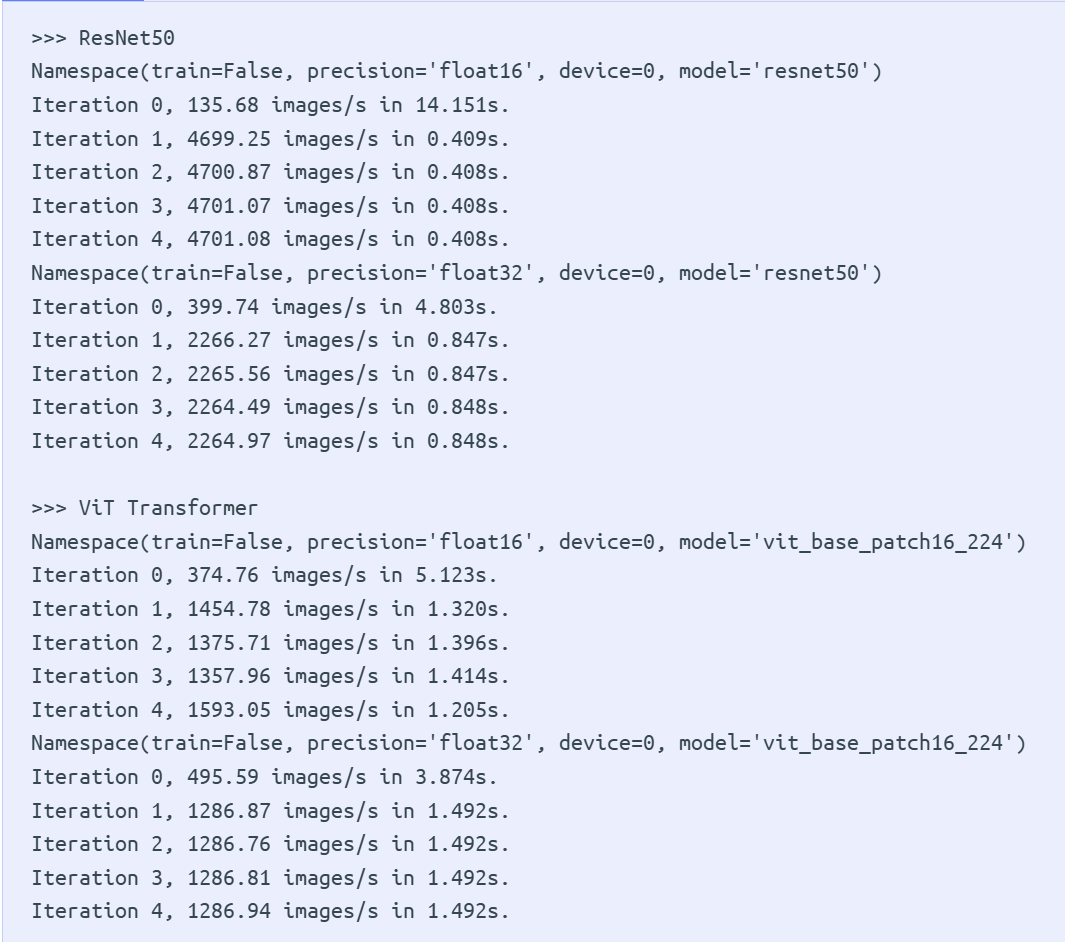
NVIDIA A100实测 data:
1. Software Ecosystem
Ascend's software ecosystem relies on CANN (Compute Architecture for Neural Networks), equivalent to NVIDIA's CUDA, currently fully open-sourced, providing full-stack tools from operator development to model optimization. In framework compatibility, PyTorch 2.1 has natively supported Ascend, allowing developers to directly install via pip install without complex adaptation. Simultaneously, Ascend is compatible with TensorFlow, PaddlePaddle, and Huawei's self-developed MindSpore framework. Worth mentioning, HuggingFace community's Transformers library has natively supported Ascend — models can run directly after download. Ascend community's ModelZoo 2.0 also provides hundreds of pretrained models, further lowering development barriers.
2. Shipments and Market Position
Ascend's shipment growth is迅猛, with market position continuously rising. According to IDC data, 2024 Huawei Ascend shipments reached 640K units, making it the only domestic vendor in China's AI chip market capable of competing with NVIDIA. Mizuho Securities predicts 2025 shipments will exceed 700K units, showing strong demand and production resilience under external sanctions. Entering 2026, industry普遍 predicts total shipments between 800K–850K units. According to Sing Tao Global Network and Bloomberg reports, Huawei's internal production plan targets are more aggressive, planning to raise Ascend product line total production (wafer-level) to 1.6 million units, with flagship 910C targeted at 600K units — approximately double that of 2025.
Behind shipment growth is Ascend's rising position in China's AI chip market. According to renowned research institution Bernstein Research's forecast, China's AI chip market格局 in 2026 will undergo a fundamental reversal: Huawei Ascend's market share is预计 to大幅 grow to 50%, becoming the absolute leader in the Chinese market; while NVIDIA's share may sharply contract from its 2025 high to 8%, affected by US sanction policies.
6.10 Ascend NPU Environment Configuration Guide, Deployment Steps, and Optimization Suggestions
The most likely hardware we can access now is Huawei's Ascend series cards. Here's a partner link: It收录了 LLM deployment tutorials tested and verified on the Ascend NPU platform, for those who need it.
6.11 Key Takeaways
- GPU architecture evolution: graphics → programmable shaders → general-purpose computing → AI acceleration
- SM/Warp/Block/Thread hierarchy is fundamental to GPU programming
- 6-layer memory hierarchy exists because speed and capacity cannot coexist — hierarchical design is the only economically viable solution
- Low precision (BF16) is the single most impactful optimization — 2× memory savings, 16× Tensor Core throughput; four mechanisms work together: hardware simplification, bandwidth savings, dedicated Tensor Cores, and parallelism boost
- Operator fusion, recomputation, memory coalescing, and tiling each attack different bottlenecks; combined they can achieve order-of-magnitude speedups
- FlashAttention V1→V2→V3: from solving IO bottleneck → parallel scheduling → computation-memory-access overlap, a paradigm of algorithm-hardware co-design
- PagedAttention transforms KV Cache from "static contiguous storage" to "dynamic paged management," achieving orders-of-magnitude memory utilization improvement
- Domestic GPUs are rising rapidly — Huawei Ascend leads deployments, Baidu Kunlun, Haiguang, Moore Threads, Tianshu Zhixin, and Alibaba T-Head each have differentiated positioning
- Roofline model guides optimization: know whether you're memory-bound or compute-bound
- GPU optimization is about managing the compute-vs-memory gap — compute grows 100,000× while memory grows 100×